SLOSE48 December   2020 DRV8434A

PRODUCTION DATA  

  1. Features
  2. Applications
  3. Description
  4. Revision History
  5. Pin Configuration and Functions
    1. 5.1 Pin Functions
  6. Specifications
    1. 6.1 Absolute Maximum Ratings
    2. 6.2 ESD Ratings
    3. 6.3 Recommended Operating Conditions
    4. 6.4 Thermal Information
    5. 6.5 Electrical Characteristics
    6. 6.6 Indexer Timing Requirements
      1. 6.6.1 Typical Characteristics
  7. Detailed Description
    1. 7.1 Overview
    2. 7.2 Functional Block Diagram
    3. 7.3 Feature Description
      1. 7.3.1 Stepper Motor Driver Current Ratings
        1. 7.3.1.1 Peak Current Rating
        2. 7.3.1.2 RMS Current Rating
        3. 7.3.1.3 Full-Scale Current Rating
      2. 7.3.2 PWM Motor Drivers
      3. 7.3.3 Microstepping Indexer
      4. 7.3.4 Controlling VREF with an MCU DAC
      5. 7.3.5 Current Regulation and Decay Mode
        1. 7.3.5.1 Smart tune Ripple Control
        2. 7.3.5.2 Blanking Time
      6. 7.3.6 Charge Pump
      7. 7.3.7 Linear Voltage Regulators
      8. 7.3.8 Logic Level, tri-level and quad-level Pin Diagrams
        1. 7.3.8.1 nFAULT Pin
      9. 7.3.9 Protection Circuits
        1. 7.3.9.1 VM Undervoltage Lockout (UVLO)
        2. 7.3.9.2 VCP Undervoltage Lockout (CPUV)
        3. 7.3.9.3 Overcurrent Protection (OCP)
        4. 7.3.9.4 Stall Detection
        5. 7.3.9.5 Open-Load Detection (OL)
        6. 7.3.9.6 Thermal Shutdown (OTSD)
        7.       Fault Condition Summary
    4. 7.4 Device Functional Modes
      1. 7.4.1 Sleep Mode (nSLEEP = 0)
      2.      43
      3. 7.4.2 Disable Mode (nSLEEP = 1, ENABLE = 0)
      4. 7.4.3 Operating Mode (nSLEEP = 1, ENABLE = Hi-Z/1)
      5. 7.4.4 nSLEEP Reset Pulse
      6.      Functional Modes Summary
  8. Application and Implementation
    1. 8.1 Application Information
    2. 8.2 Typical Application
      1. 8.2.1 Design Requirements
      2. 8.2.2 Detailed Design Procedure
        1. 8.2.2.1 Stepper Motor Speed
        2. 8.2.2.2 Current Regulation
        3. 8.2.2.3 Decay Mode
        4. 8.2.2.4 Application Curves
        5. 8.2.2.5 Thermal Application
          1. 8.2.2.5.1 Power Dissipation
          2. 8.2.2.5.2 Conduction Loss
          3. 8.2.2.5.3 Switching Loss
          4. 8.2.2.5.4 Power Dissipation Due to Quiescent Current
          5. 8.2.2.5.5 Total Power Dissipation
          6. 8.2.2.5.6 Device Junction Temperature Estimation
  9. Power Supply Recommendations
    1. 9.1 Bulk Capacitance
  10. 10Layout
    1. 10.1 Layout Guidelines
    2. 10.2 Layout Example
  11. 11Device and Documentation Support
    1. 11.1 Receiving Notification of Documentation Updates
    2. 11.2 Support Resources
    3. 11.3 Trademarks
    4. 11.4 Electrostatic Discharge Caution
    5. 11.5 Glossary
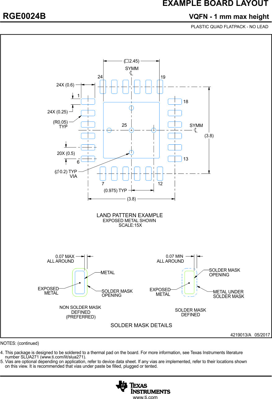
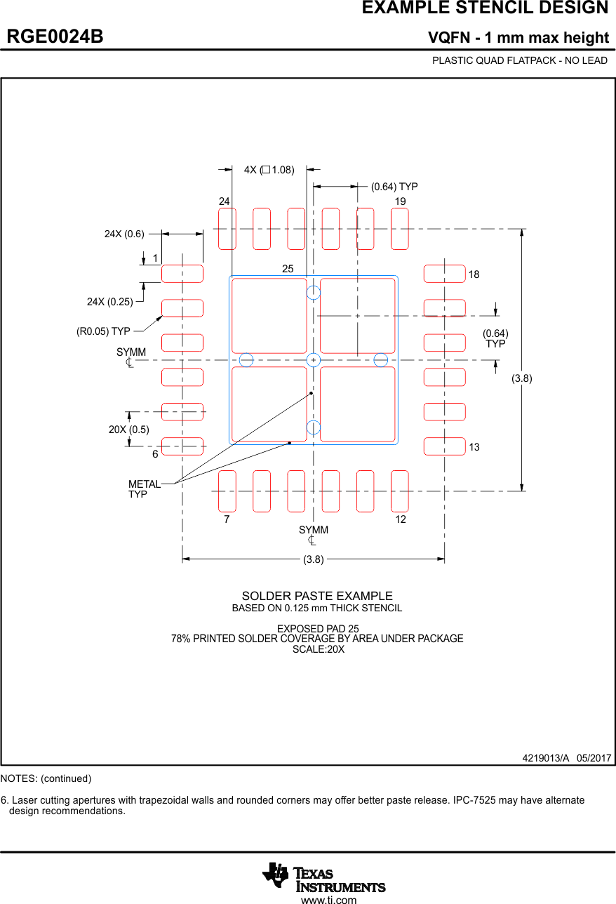
  12. 12Mechanical, Packaging, and Orderable Information

Package Options

Mechanical Data (Package|Pins)
Thermal pad, mechanical data (Package|Pins)
Orderable Information

Mechanical, Packaging, and Orderable Information

The following pages include mechanical, packaging, and orderable information. This information is the most current data available for the designated devices. This data is subject to change without notice and revision of this document. For browser-based versions of this data sheet, refer to the left-hand navigation.

GUID-1628D1D6-0D8F-48C1-858D-7A4FFB02EB48-low.gif
GUID-3BF43EA7-0453-4301-8B3B-2CA6AEA85594-low.gif
GUID-A3111556-BA3C-4F07-8A35-1B846C340BEF-low.gif
GUID-F18EE168-A1D7-45B0-A6A3-6FDC2640BE58-low.gif
GUID-DA0214D2-3C29-47E1-AE0B-B5B16084A2FD-low.gif
GUID-3C32B39C-C95C-4ABF-96DF-E0D8954A3BD1-low.gif