SLOSE48 December 2020 DRV8434A
PRODUCTION DATA
- 1 Features
- 2 Applications
- 3 Description
- 4 Revision History
- 5 Pin Configuration and Functions
- 6 Specifications
-
7 Detailed Description
- 7.1 Overview
- 7.2 Functional Block Diagram
- 7.3
Feature Description
- 7.3.1 Stepper Motor Driver Current Ratings
- 7.3.2 PWM Motor Drivers
- 7.3.3 Microstepping Indexer
- 7.3.4 Controlling VREF with an MCU DAC
- 7.3.5 Current Regulation and Decay Mode
- 7.3.6 Charge Pump
- 7.3.7 Linear Voltage Regulators
- 7.3.8 Logic Level, tri-level and quad-level Pin Diagrams
- 7.3.9 Protection Circuits
- 7.4 Device Functional Modes
- 8 Application and Implementation
- 9 Power Supply Recommendations
- 10Layout
- 11Device and Documentation Support
- 12Mechanical, Packaging, and Orderable Information
Package Options
Mechanical Data (Package|Pins)
Thermal pad, mechanical data (Package|Pins)
- RGE|24
Orderable Information
8.2.2.1 Stepper Motor Speed
The first step in configuring the DRV8434A requires the desired motor speed and microstepping level. If the target application requires a constant speed, then a square wave with frequency ƒstep must be applied to the STEP pin. If the target motor speed is too high, the motor does not spin. Make sure that the motor can support the target speed. Use Equation 1 to calculate ƒstep for a desired motor speed (v), microstepping level (nm), and motor full step angle (θstep)
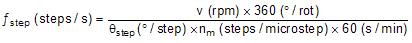
The value of θstep can be found in the stepper motor data sheet, or written on the motor. For example, the motor in this application is required to rotate at 1.8°/step for a target of 18.75 rpm at 1/8 microstep mode. Using Equation 1, ƒstep can be calculated as 500 Hz.
The microstepping level is set by the M0 and M1 pins and can be any of the settings listed in Table 8-2. Higher microstepping results in a smoother motor motion and less audible noise, but requires a higher ƒstep to achieve the same motor speed.
M0 | M1 | STEP MODE |
|---|---|---|
0 | 0 | Full step (2-phase excitation) with 100% current |
0 | 330 kΩ to GND | Full step (2-phase excitation) with 71% current |
1 |
0 | Non-circular 1/2 step |
Hi-Z |
0 | 1/2 step |
0 |
1 | 1/4 step |
1 |
1 | 1/8 step |
Hi-Z |
1 | 1/16 step |
0 | Hi-Z | 1/32 step |
Hi-Z |
330 kΩ to GND | 1/64 step |
| Hi-Z |
Hi-Z | 1/128 step |
1 | Hi-Z | 1/256 step |