SLOSE70 December 2020 DRV8434S
PRODUCTION DATA
- 1 Features
- 2 Applications
- 3 Description
- 4 Revision History
- 5 Pin Configuration and Functions
- 6 Specifications
-
7 Detailed Description
- 7.1 Overview
- 7.2 Functional Block Diagram
- 7.3
Feature Description
- 7.3.1 Stepper Motor Driver Current Ratings
- 7.3.2 PWM Motor Drivers
- 7.3.3 Microstepping Indexer
- 7.3.4 Controlling VREF with an MCU DAC
- 7.3.5 Current Regulation
- 7.3.6
Decay Modes
- 7.3.6.1 Slow Decay for Increasing and Decreasing Current
- 7.3.6.2 Slow Decay for Increasing Current, Mixed Decay for Decreasing Current
- 7.3.6.3 Slow Decay for Increasing Current, Fast Decay for Decreasing current
- 7.3.6.4 Mixed Decay for Increasing and Decreasing Current
- 7.3.6.5 Smart tune Dynamic Decay
- 7.3.6.6 Smart tune Ripple Control
- 7.3.7 PWM OFF Time
- 7.3.8 Blanking time
- 7.3.9 Charge Pump
- 7.3.10 Linear Voltage Regulators
- 7.3.11 Logic Level, tri-level and quad-level Pin Diagrams
- 7.3.12 Protection Circuits
- 7.4 Device Functional Modes
- 7.5 Programming
- 7.6 Register Maps
- 8 Application and Implementation
- 9 Power Supply Recommendations
- 10Layout
- 11Device and Documentation Support
- 12Mechanical, Packaging, and Orderable Information
Package Options
Mechanical Data (Package|Pins)
Thermal pad, mechanical data (Package|Pins)
- RGE|24
Orderable Information
7.3.12.1 VM Undervoltage Lockout (UVLO)
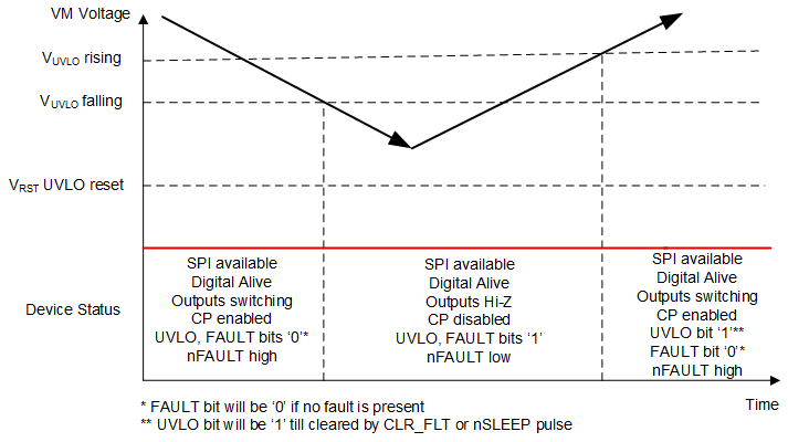
 Figure 7-19 Supply Voltage Ramp Profile
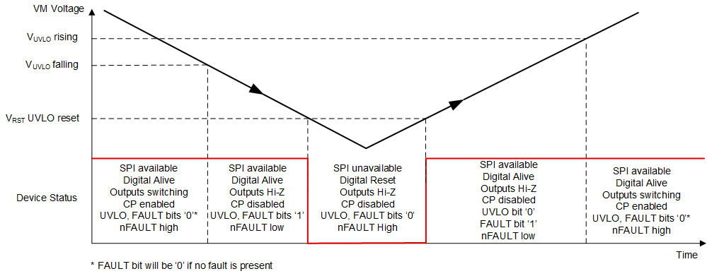
 Figure 7-20 Supply Voltage Ramp Profile
If at any time the voltage on the VM pin falls below the UVLO falling threshold voltage, all the outputs are disabled (High-Z) and the charge pump (CP) is disabled. Normal operation resumes (motor driver and charge pump) when the VM voltage recovers above the UVLO rising threshold voltage.
When the voltage on the VM pin falls below the UVLO falling threshold voltage (4.25 V typical), but is above the VM UVLO reset voltage (VRST, 3.9 V maximum), SPI communication is available, the digital core of the device is active, the FAULT and UVLO bits are made high in the SPI registers and the nFAULT pin is driven low, as shown in Figure 7-19. From this condition, if the VM voltage recovers above the UVLO rising threshold voltage (4.35 V typical), nFAULT pin is released (is pulled-up to the external voltage), and the FAULT bit is reset, but the UVLO bit remains latched high until cleared through the CLR_FLT bit or an nSLEEP reset pulse.
When the voltage on the VM pin falls below the VM UVLO reset voltage (VRST, 3.9 V maximum), SPI communication is unavailable, the digital core is shutdown, the FAULT and UVLO bits are low and the nFAULT pin is high. During a subsequent power-up, when the VM voltage exceeds the VRST voltage, the digital core comes alive, UVLO bit stays low but the FAULT bit is made high; and the nFAULT pin is pulled low, as shown in Figure 7-20. When the VM voltage exceeds the VM UVLO rising threshold, FAULT bit is reset, UVLO bit stays low and the nFAULT pin is pulled high.