SLOSE70 December 2020 DRV8434S
PRODUCTION DATA
- 1 Features
- 2 Applications
- 3 Description
- 4 Revision History
- 5 Pin Configuration and Functions
- 6 Specifications
-
7 Detailed Description
- 7.1 Overview
- 7.2 Functional Block Diagram
- 7.3
Feature Description
- 7.3.1 Stepper Motor Driver Current Ratings
- 7.3.2 PWM Motor Drivers
- 7.3.3 Microstepping Indexer
- 7.3.4 Controlling VREF with an MCU DAC
- 7.3.5 Current Regulation
- 7.3.6
Decay Modes
- 7.3.6.1 Slow Decay for Increasing and Decreasing Current
- 7.3.6.2 Slow Decay for Increasing Current, Mixed Decay for Decreasing Current
- 7.3.6.3 Slow Decay for Increasing Current, Fast Decay for Decreasing current
- 7.3.6.4 Mixed Decay for Increasing and Decreasing Current
- 7.3.6.5 Smart tune Dynamic Decay
- 7.3.6.6 Smart tune Ripple Control
- 7.3.7 PWM OFF Time
- 7.3.8 Blanking time
- 7.3.9 Charge Pump
- 7.3.10 Linear Voltage Regulators
- 7.3.11 Logic Level, tri-level and quad-level Pin Diagrams
- 7.3.12 Protection Circuits
- 7.4 Device Functional Modes
- 7.5 Programming
- 7.6 Register Maps
- 8 Application and Implementation
- 9 Power Supply Recommendations
- 10Layout
- 11Device and Documentation Support
- 12Mechanical, Packaging, and Orderable Information
Package Options
Mechanical Data (Package|Pins)
Thermal pad, mechanical data (Package|Pins)
- RGE|24
Orderable Information
7.3.6.5 Smart tune Dynamic Decay
The smart tune current regulation schemes are advanced current-regulation control methods compared to traditional fixed off-time current regulation schemes. Smart tune current regulation schemes help the stepper motor driver adjust the decay scheme based on factors such as:
- Motor winding resistance and inductance
- Motor aging effects
- Motor dynamic speed and load
- Motor supply voltage variation
- Motor back-EMF difference on rising and falling steps
- Step transitions
- Low-current versus high-current dI/dt
The device provides two different smart tune current regulation modes, named smart tune Dynamic Decay and smart tune Ripple Control.
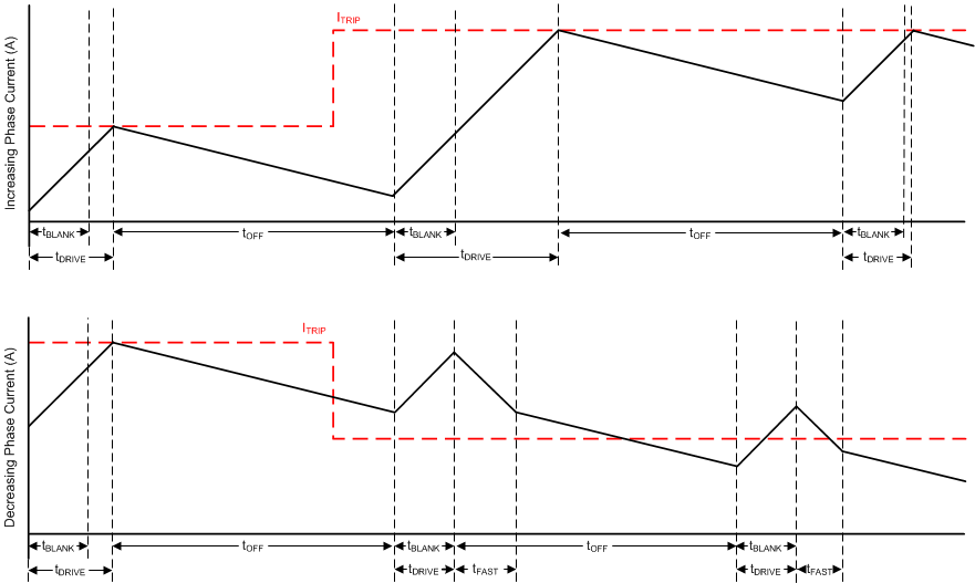
 Figure 7-12 Smart tune Dynamic Decay Mode
Smart tune Dynamic Decay greatly simplifies the decay mode selection by automatically configuring the decay mode between slow, mixed, and fast decay. In mixed decay, smart tune dynamically adjusts the fast decay percentage of the total mixed decay time. This feature eliminates motor tuning by automatically determining the best decay setting that results in the lowest ripple for a motor.
The decay mode setting is optimized iteratively each PWM cycle. If the motor current overshoots the target trip level, then the decay mode becomes more aggressive (increases fast decay percentage) on the next cycle to prevent regulation loss. Should a long drive time must occur to reach the target trip level, the decay mode becomes less aggressive (decreases fast decay percentage) on the next cycle to operate with less ripple more efficiently. With decreasing current steps, smart tune Dynamic Decay automatically switches to fast decay to reach the next current step quickly.
Smart tune Dynamic Decay is best suited for applications that require lowest possible current ripple, at the same time maintain a fixed frequency with the current regulation scheme.