SLVSFF0B June   2020  – July 2022 DRV8436E

PRODUCTION DATA  

  1. Features
  2. Applications
  3. Description
  4. Revision History
    1.     Device Options
  5. Pin Configuration and Functions
  6. Specifications
    1. 6.1 Absolute Maximum Ratings
    2. 6.2 ESD Ratings
    3. 6.3 Recommended Operating Conditions
    4. 6.4 Thermal Information
    5. 6.5 Electrical Characteristics
    6. 6.6 Typical Characteristics
  7. Detailed Description
    1. 7.1 Overview
    2. 7.2 Functional Block Diagrams
    3. 7.3 Feature Description
      1. 7.3.1 PWM Motor Drivers
      2. 7.3.2 Bridge Control
      3. 7.3.3 Current Regulation
      4. 7.3.4 Decay Modes
        1. 7.3.4.1 Slow Decay
        2. 7.3.4.2 Mixed Decay
        3. 7.3.4.3 Fast Decay
        4. 7.3.4.4 Smart tune Dynamic Decay
        5. 7.3.4.5 Blanking time
      5. 7.3.5 Charge Pump
      6. 7.3.6 Linear Voltage Regulators
      7. 7.3.7 Logic and Quad-Level Pin Diagrams
        1. 7.3.7.1 nFAULT Pin
      8. 7.3.8 Protection Circuits
        1. 7.3.8.1 VM Undervoltage Lockout (UVLO)
        2. 7.3.8.2 VCP Undervoltage Lockout (CPUV)
        3. 7.3.8.3 Overcurrent Protection (OCP)
        4. 7.3.8.4 Thermal Shutdown (OTSD)
        5. 7.3.8.5 36
    4. 7.4 Device Functional Modes
      1. 7.4.1 Sleep Mode (nSLEEP = 0)
      2. 7.4.2 Operating Mode (nSLEEP = 1)
      3. 7.4.3 Functional Modes Summary
  8. Application and Implementation
    1. 8.1 Application Information
    2. 8.2 Primary Application
      1. 8.2.1 Design Requirements
      2. 8.2.2 Detailed Design Procedure
        1. 8.2.2.1 Current Regulation
    3. 8.3 Typical Application
      1. 8.3.1 Design Requirements
      2. 8.3.2 Detailed Design Procedure
        1. 8.3.2.1 Current Regulation
        2. 8.3.2.2 Stepper Motor Speed
        3. 8.3.2.3 Decay Modes
  9. Power Supply Recommendations
    1. 9.1 Bulk Capacitance
  10. 10Layout
    1. 10.1 Layout Guidelines
    2. 10.2 Layout Example
  11. 11Device and Documentation Support
    1. 11.1 Documentation Support
      1. 11.1.1 Related Documentation
    2. 11.2 Related Links
    3. 11.3 Receiving Notification of Documentation Updates
    4. 11.4 Community Resources
    5. 11.5 Trademarks
  12. 12Mechanical, Packaging, and Orderable Information

Package Options

Mechanical Data (Package|Pins)
Thermal pad, mechanical data (Package|Pins)
Orderable Information

Decay Modes

During PWM current chopping, the H-bridge is enabled to drive through the motor winding until the PWM current chopping threshold is reached. This is shown in Figure 7-5, Item 1.

Once the chopping current threshold is reached, the H-bridge can operate in two different states, fast decay or slow decay. In fast decay mode, once the PWM chopping current level has been reached, the H-bridge reverses state to allow winding current to flow in a reverse direction. Fast decay mode is shown in Figure 7-5, item 2. In slow decay mode, winding current is re-circulated by enabling both of the low-side FETs in the bridge. This is shown in Figure 7-5, Item 3.
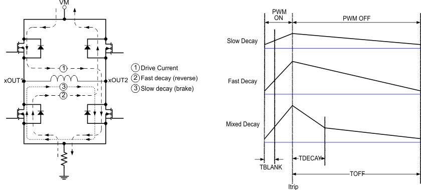
GUID-09B8F977-C8E5-4B76-B195-C70E257891D9-low.gifFigure 7-5 Decay Modes

The decay mode is selected by setting the quad-level ADECAY and BDECAY pins as shown in Table 7-5.

Table 7-5 Decay Mode Settings
xDECAYDECAY MODE
0Smart tune Dynamic Decay
330k to GNDSlow decay
Hi-ZMixed decay: 30% fast
1Fast decay

The ADECAY pin sets the decay mode for H-bridge A (AOUT1, AOUT2), and the BDECAY pin sets the decay mode for H-bridge B (BOUT1, BOUT2).