SLVSFF0B June   2020  – July 2022 DRV8436E

PRODUCTION DATA  

  1. Features
  2. Applications
  3. Description
  4. Revision History
    1.     Device Options
  5. Pin Configuration and Functions
  6. Specifications
    1. 6.1 Absolute Maximum Ratings
    2. 6.2 ESD Ratings
    3. 6.3 Recommended Operating Conditions
    4. 6.4 Thermal Information
    5. 6.5 Electrical Characteristics
    6. 6.6 Typical Characteristics
  7. Detailed Description
    1. 7.1 Overview
    2. 7.2 Functional Block Diagrams
    3. 7.3 Feature Description
      1. 7.3.1 PWM Motor Drivers
      2. 7.3.2 Bridge Control
      3. 7.3.3 Current Regulation
      4. 7.3.4 Decay Modes
        1. 7.3.4.1 Slow Decay
        2. 7.3.4.2 Mixed Decay
        3. 7.3.4.3 Fast Decay
        4. 7.3.4.4 Smart tune Dynamic Decay
        5. 7.3.4.5 Blanking time
      5. 7.3.5 Charge Pump
      6. 7.3.6 Linear Voltage Regulators
      7. 7.3.7 Logic and Quad-Level Pin Diagrams
        1. 7.3.7.1 nFAULT Pin
      8. 7.3.8 Protection Circuits
        1. 7.3.8.1 VM Undervoltage Lockout (UVLO)
        2. 7.3.8.2 VCP Undervoltage Lockout (CPUV)
        3. 7.3.8.3 Overcurrent Protection (OCP)
        4. 7.3.8.4 Thermal Shutdown (OTSD)
        5. 7.3.8.5 36
    4. 7.4 Device Functional Modes
      1. 7.4.1 Sleep Mode (nSLEEP = 0)
      2. 7.4.2 Operating Mode (nSLEEP = 1)
      3. 7.4.3 Functional Modes Summary
  8. Application and Implementation
    1. 8.1 Application Information
    2. 8.2 Primary Application
      1. 8.2.1 Design Requirements
      2. 8.2.2 Detailed Design Procedure
        1. 8.2.2.1 Current Regulation
    3. 8.3 Typical Application
      1. 8.3.1 Design Requirements
      2. 8.3.2 Detailed Design Procedure
        1. 8.3.2.1 Current Regulation
        2. 8.3.2.2 Stepper Motor Speed
        3. 8.3.2.3 Decay Modes
  9. Power Supply Recommendations
    1. 9.1 Bulk Capacitance
  10. 10Layout
    1. 10.1 Layout Guidelines
    2. 10.2 Layout Example
  11. 11Device and Documentation Support
    1. 11.1 Documentation Support
      1. 11.1.1 Related Documentation
    2. 11.2 Related Links
    3. 11.3 Receiving Notification of Documentation Updates
    4. 11.4 Community Resources
    5. 11.5 Trademarks
  12. 12Mechanical, Packaging, and Orderable Information

Package Options

Mechanical Data (Package|Pins)
Thermal pad, mechanical data (Package|Pins)
Orderable Information

Charge Pump

A charge pump is integrated to supply a high-side N-channel MOSFET gate-drive voltage. The charge pump requires a capacitor between the VM and VCP pins to act as the storage capacitor. Additionally a ceramic capacitor is required between the CPH and CPL pins to act as the flying capacitor.
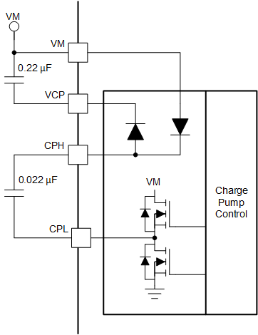
GUID-933B56D1-75BF-479F-96D1-666A44C30415-low.gifFigure 7-10 Charge Pump Block Diagram