SLVSCX5B March 2015 – July 2015 DRV8701
PRODUCTION DATA.
- 1 Features
- 2 Applications
- 3 Description
- 4 Revision History
- 5 Pin Configuration and Functions
- 6 Specifications
-
7 Detailed Description
- 7.1 Overview
- 7.2 Functional Block Diagram
- 7.3
Feature Description
- 7.3.1 Bridge Control
- 7.3.2 Half-Bridge Operation
- 7.3.3 Current Regulation
- 7.3.4 Amplifier Output SO
- 7.3.5 PWM Motor Gate Drivers
- 7.3.6 IDRIVE Pin
- 7.3.7 Dead Time
- 7.3.8 Propagation Delay
- 7.3.9 Overcurrent VDS Monitor
- 7.3.10 Charge Pump
- 7.3.11 LDO Voltage Regulators
- 7.3.12 Gate Drive Clamp
- 7.3.13 Protection Circuits
- 7.3.14 Reverse Supply Protection
- 7.4 Device Functional Modes
- 8 Application and Implementation
- 9 Power Supply Recommendations
- 10Layout
- 11Device and Documentation Support
- 12Mechanical, Packaging, and Orderable Information
Package Options
Mechanical Data (Package|Pins)
- RGE|24
Thermal pad, mechanical data (Package|Pins)
Orderable Information
7 Detailed Description
7.1 Overview
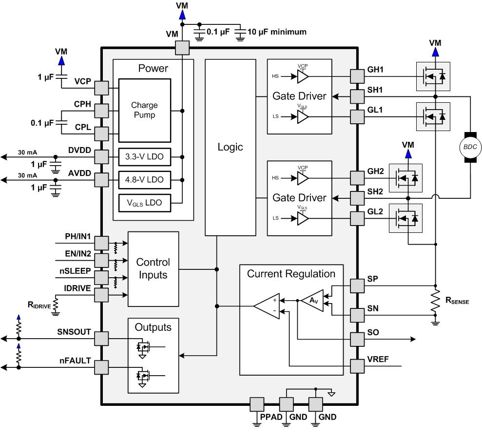
The DRV8701 is an H-bridge gate driver (also called a pre-driver or controller). The device integrates FET gate drivers in order to control four external NMOS FETs. The device can be powered with a supply voltage between 5.9 and 45 V.
A simple PH/EN (DRV8701E) or PWM (DRV8701P) interface allows interfacing to the controller circuit.
A low-power sleep mode is included, which can be enabled using the nSLEEP pin.
The gate drive strength can be adjusted to optimize a system for a given FET without adding external resistors in series with the FET gates. The IDRIVE pin allows for selection of the peak current driven into the external FET gate. Both the high-side and low-side FETs are driven with a VGS of 9.5 V nominally when VM > 12 V. At lower VM voltages, the VGS is reduced. The high-side gate drive voltage is generated using a doubler-architecture charge pump that regulates to VM + 9.5 V.
This device greatly reduces the component count of discrete motor driver systems by integrating the necessary FET drive circuitry into a single device. In addition, the DRV8701 adds protection features above traditional discrete implementations: UVLO, OCP, pre-driver faults, and thermal shutdown.
A start-up (inrush) or running current limitation is built in using a fixed time-off current chopping scheme. The chopping current level is set by choosing the sense resistor value and by setting a voltage on the VREF pin.
A shunt amplifier output is provided for accurate current measurements by the system controller. The SO pin outputs a voltage that is 20 times the voltage seen across the sense resistor.
7.2 Functional Block Diagram
7.3 Feature Description
7.3.1 Bridge Control
The DRV8701E is controlled using a PH/EN interface. The following logic table (Table 1) gives the full H-bridge state when driving a single brushed DC motor. Note that Table 1 does not take into account the current control built into the DRV8701E. Positive current is defined in the direction of xOUT1 → xOUT2.
Table 1. DRV8701E (PH/EN) Control Interface
| nSLEEP | EN | PH | SH1 | SH2 | AVDD/DVDD | Description |
|---|---|---|---|---|---|---|
| 0 | X | X | High-Z | High-Z | Disabled | Sleep mode; H-bridge disabled High-Z |
| 1 | 0 | X | L | L | Enabled | Brake, low-side slow decay |
| 1 | 1 | 0 | L | H | Enabled | Reverse drive (current SH2 → SH1) |
| 1 | 1 | 1 | H | L | Enabled | Forward drive (current SH1 → SH2) |
The DRV8701P is controlled using a PWM interface (IN1/IN2). The following logic table (Table 2) gives the full H-bridge state when driving a single brushed DC motor. Note that Table 2 does not take into account the current control built into the DRV8701P. Positive current is defined in the direction of xOUT1 → xOUT2.
Table 2. DRV8701P (PWM) Control Interface
| nSLEEP | IN1 | IN2 | SH1 | SH2 | AVDD/DVDD | Description |
|---|---|---|---|---|---|---|
| 0 | X | X | High-Z | High-Z | Disabled | Sleep mode; H-bridge disabled High-Z |
| 1 | 0 | 0 | High-Z | High-Z | Enabled | Coast; H-bridge disabled High-Z |
| 1 | 0 | 1 | L | H | Enabled | Reverse (current SH2 → SH1) |
| 1 | 1 | 0 | H | L | Enabled | Forward (current SH1 → SH2) |
| 1 | 1 | 1 | L | L | Enabled | Brake; low-side slow decay |
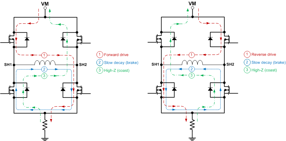 Figure 19. H-Bridge Operational States
7.3.2 Half-Bridge Operation
The DRV8701 can be used to drive only a single half-bridge instead of a full H-bridge. To operate in this mode, leave GH1 and GL1 disconnected. Also, connect a 1/10 W, 330-Ω 5% resistor from SH1 to GND.
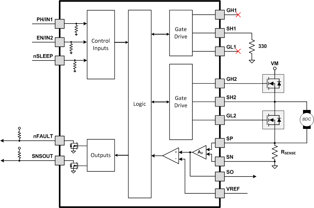 Figure 20. Half-H Bridge Operation Mode
For the DRV8701E, this mode is controlled by tying the PH pin low. Table 3 gives the control scheme. EN = 1 enables the high-side FET, and EN = 0 enables the low-side FET. EN = 1 and PH = 1 is an invalid state.
Table 3. DRV8701E (PH/EN) Control Interface for Half-H Bridge Mode
| nSLEEP | EN | PH | SH2 | AVDD/DVDD | Description |
|---|---|---|---|---|---|
| 0 | X | X | High-Z | Disabled | Sleep mode; disabled High-Z |
| 1 | 0 | X | L | Enabled | Brake, low-side slow decay |
| 1 | 1 | 0 | H | Enabled | Drive (Current SH2 → GND) |
| 1 | 1 | 1 | Invalid state | ||
For the DRV8701P, Table 4 gives the control scheme. IN1 = 1 and IN2 = 0 is an invalid state.
Table 4. DRV8701P (PWM) Control Interface for Half-H Bridge Mode
| nSLEEP | IN1 | IN2 | SH2 | AVDD/DVDD | Description |
|---|---|---|---|---|---|
| 0 | X | X | High-Z | Disabled | Sleep mode; disabled High-Z |
| 1 | 0 | 0 | High-Z | Enabled | Coast; disabled High-Z |
| 1 | 0 | 1 | H | Enabled | Drive (current SH2 → GND) |
| 1 | 1 | 0 | Invalid state | ||
| 1 | 1 | 1 | L | Enabled | Brake; low-side slow decay |
7.3.3 Current Regulation
The maximum current through the motor winding is regulated by a fixed off-time PWM current regulation, or current chopping. When an H-bridge is enabled in forward or reverse drive, current rises through the winding at a rate dependent on the DC voltage and inductance of the winding. After the current hits the current chopping threshold, the bridge enters a brake (low-side slow decay) mode until tOFF has expired.
Note that immediately after the current is enabled, the voltage on the SP pin is ignored for a period of time (tBLANK) before enabling the current sense circuitry.
The PWM chopping current is set by a comparator which compares the voltage across a current sense resistor connected to the SP pin, multiplied by a factor of AV, with a reference voltage from the VREF pin. The factor AV is the shunt amplifier gain, which is 20 V/V in the DRV8701.
The chopping current is calculated as follows:

Example: If a 50 mΩ sense resistor is used and VREF = 3.3 V, the full-scale chopping current will be 3.25 A. AV is 20 V/V and VOFF is assumed to be 50 mV in this example.
For DC motors, current regulation is generally used to limit the start-up and stall current of the motor. If the current regulation feature is not needed, it can be disabled by tying VREF directly to AVDD and tying SP and SN to GND.
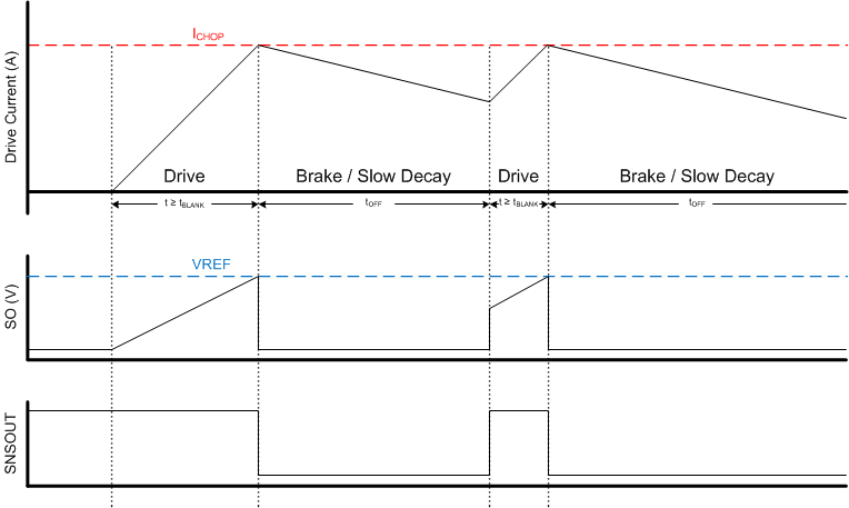 Figure 21. Sense Amplifier and Current Chopping Operation
During brake mode (slow decay), current is recirculated through the low-side FETs. Because current is not flowing through the sense resistor, SO does not represent the motor current.
7.3.4 Amplifier Output SO
The SO pin on the DRV8701 outputs an analog voltage equal to the voltage seen across the SP and SN pins multiplied by AV. The factor AV is the shunt amplifier gain, which is 20 V/V in the DRV8701. SO is only valid during forward or reverse drive. The H-bridge current is approximately equal to:

When SP and SN are 0 V, SO outputs the amplifier offset voltage VOFF. No capacitor is required on the SO pin.
 Figure 22. Sense Amplifier Diagram
If the voltage across SP and SN exceeds 1 V, then the DRV8701 flags an overcurrent condition.
The SO pin can source up to 5 mA of current. If the pin is shorted to GND, or if a higher-current load is driven by this pin, the output acts as a constant-current source. The output voltage is not representative of the H-bridge current in this state.
This shunt amplifier feature can be disabled by tying the SP and SN pins to GND. When the amplifier is disabled, current regulation is also disabled.
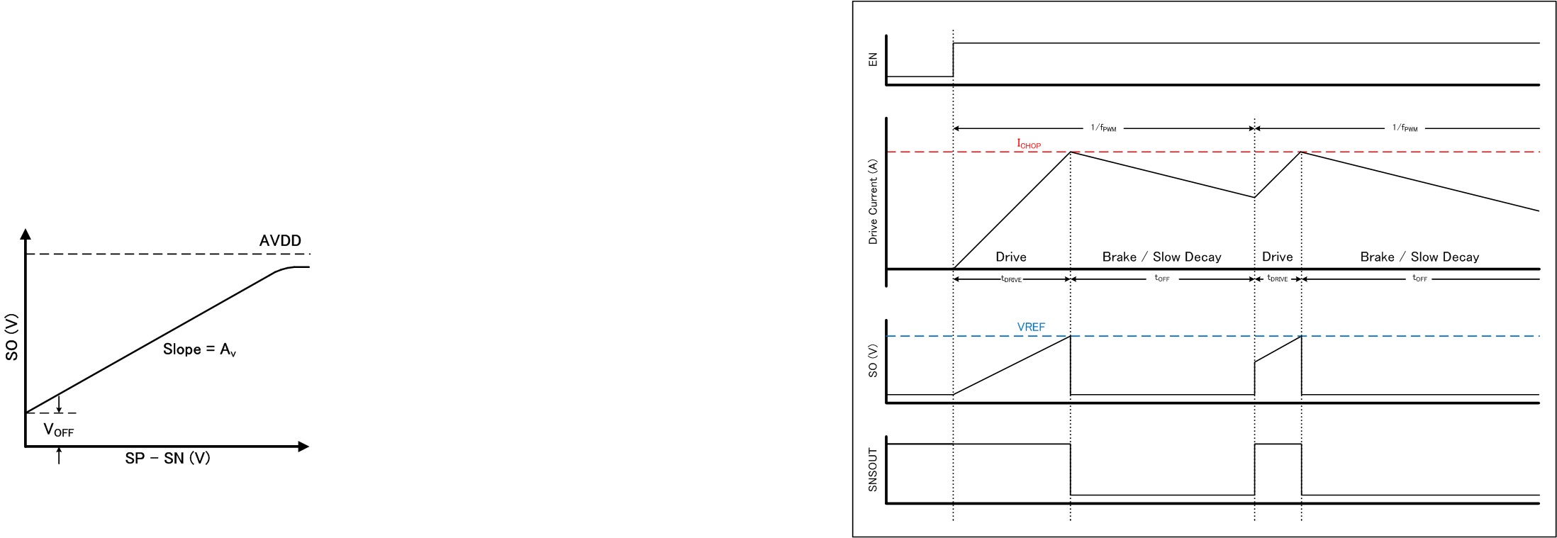 Figure 23. Sense Amplifier Output
7.3.4.1 SNSOUT
The SNSOUT pin of the DRV8701 indicates when the device is in current chopping mode. When the driver is in a slow decay mode caused by internal PWM current chopping (ICHOP threshold hit), the open-drain SNSOUT output is pulled low. If the current regulation is disabled, then the SNSOUT pin will be high-Z.
Note that if the H-bridge is put into a slow decay mode using the inputs (PH/EN or IN1/IN2), then SNSOUT is not pulled low.
During forward or reverse drive mode, SNSOUT is high until the DRV8701 is internally forced into current chopping. If the drive current rises above ICHOP, the driver enters a brake mode (low-side slow decay). The SNSOUT pin will be pulled low during this current chopping brake mode. After the driver is re-enabled, the SNSOUT pin is released high-Z and the drive mode is restarted.
7.3.5 PWM Motor Gate Drivers
The DRV8701 contains gate drivers for a single H-bridge with external NMOS FETs. Figure 24 shows a block diagram of the gate driver circuitry.
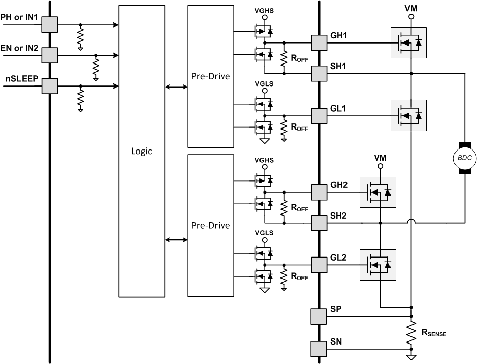 Figure 24. PWM Motor Gate Drivers
Gate drivers inside the DRV8701 directly drive N-channel MOSFETs, which drive the motor current. The high-side gate drive is supplied by the charge pump, while the low-side gate drive voltage is generated by an internal regulator.
The peak drive current of the gate drivers is adjustable through the IDRIVE pin. Peak source currents may be set to 6, 12.5, 25, 100, or 150 mA. The peak sink current is approximately 2× the peak source current. Adjusting the peak current changes the output slew rate, which also depends on the FET input capacitance and gate charge.
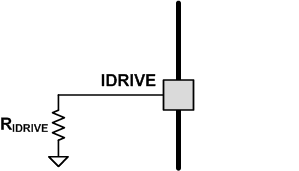
The peak drive current is selected by setting the value of the RIDRIVE resistor on the IDRIVE pin or by forcing a voltage onto the IDRIVE pin (see Table 6 for details).
Fast switching times can cause extra voltage noise on VM and GND. This can be especially due to a relatively slow reverse-recovery time of the low-side body diode, where it conducts reverse-bias momentarily, being similar to shoot-through. Slow switching times can cause excessive power dissipation since the external FETs take a longer time to turn on and turn off.
When changing the state of the output, the peak current (IDRIVE) is applied for a short drive period (tDRIVE) to charge the gate capacitance. After this time, a weaker current source (IHOLD) is used to keep the gate at the desired state. When selecting the gate drive strength for a given external FET, the selected current must be high enough to fully charge and discharge the gate during tDRIVE, or excessive power will be dissipated in the FET.
During high-side turn-on, the low-side gate is pulled low with a strong pull-down (ISTRONG). This prevents the low-side FET QGS from charging and keeps the FET off, even when there is fast switching at the outputs.
The pre-driver circuits include enforcement of a dead time in analog circuitry, which prevents the high-side and low-side FETs from conducting at the same time. When switching FETs on, this handshaking prevents the high- or low-side FET from turning on until the opposite FET has been turned off.
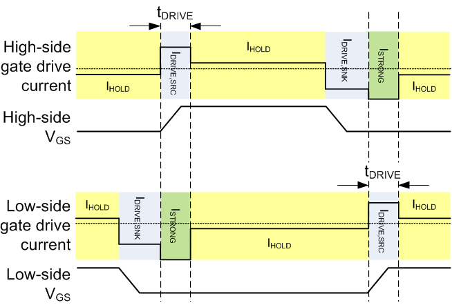 Figure 25. Gate Driver Output to Control External FETs
QGD Miller charge
When a FET gate is turned on, three different capacitances must be charged.
- QGS – Gate-to-source charge
- QGD – Gate-to-drain charge (miller charge)
- Remaining QG
The FET output is slewing primarily during the QGD charge.
 Figure 26. Example FET Gate Charging Profile
7.3.6 IDRIVE Pin
The rise and fall times of the H-bridge output (SHx pins) can be adjusted by setting the IDRIVE resistor value or forcing a voltage onto the IDRIVE pin. The FET gate voltage ramps faster if a higher IDRIVE setting is chosen. The FET gate ramp directly affects the H-bridge output rise and fall time.
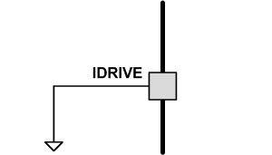
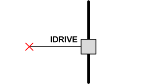
Tying IDRIVE to GND selects the lowest drive setting of 6-mA source and 12.5-mA sink. If this pin is left unconnected, then the 100-mA source and 200-mA sink setting are selected.
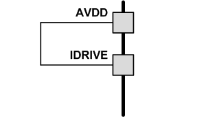
If IDRIVE is shorted to AVDD, then the VDS OCP monitor on the high-side FETs is disabled. In this setting, the gate driver is configured as 25-mA source and 50-mA sink.
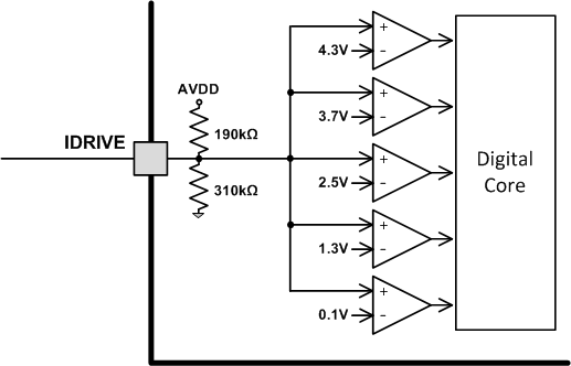 Figure 27. IDRIVE Pin Internal Circuitry
Table 5. IDRIVE Pin Configuration Settings
| IDRIVE Resistance | IDRIVE Voltage | Source Current (IDRIVE,SRC) | Sink Current (IDRIVE,SNK) | HS OCP Monitor |
|---|---|---|---|---|
| <1 kΩ to GND | GND | 6 mA | 12.5 mA | ON |
| 33 kΩ ±5% to GND | 0.7 V ±5% | 12.5 mA | 25 mA | ON |
| 200 kΩ ±5% to GND | 2 V ±5% | 25 mA | 50 mA | ON |
| >500 kΩ to GND, High-Z | 3 V ±5% | 100 mA | 200 mA | ON |
| 68 kΩ ±5% to AVDD | 4 V ±5% | 150 mA | 300 mA | ON |
| <1 kΩ to AVDD | AVDD | 25 mA | 50 mA | OFF |
Table 6. IDRIVE Pin Resistor Settings
| <1 kΩ to GND | 33 kΩ ±5% to GND 200 kΩ ±5% to GND |
>500 kΩ to GND, High-Z | 68 kΩ ±5% to AVDD | <1 kΩ to AVDD |
|---|---|---|---|---|
 |
 |
 |
 |
 |
| IDRIVE | IDRIVE | IDRIVE | IDRIVE | IDRIVE |
| 6 / 12.5 mA | 12.5 / 25 mA (33 kΩ) 25 / 50 mA (200 kΩ) |
100 / 200 mA | 150 / 300 mA | 25 / 50 mA HS OCP monitor off |
7.3.7 Dead Time
Dead time (tDEAD) is measured as the time when SHx is High-Z between turning off one of the H-bridge FETs and turning on the other. For example, the output is High-Z between turning off the high-side FET and turning on the low-side FET.
The DRV8701 inserts a digital dead time of approximately 150 ns. The total dead time also includes the FET gate turn-on time.
The total dead time is dependent on the IDRIVE resistor setting because a portion of the FET gate ramp (GHx and GLx pins) includes the observable dead time.
7.3.8 Propagation Delay
The propagation delay time (tDELAY) is measured as the time between an input edge to an output change. This time is composed of two parts: an input deglitch time and output slewing delay. The input deglitcher prevents noise on the input pins from affecting the output state.
The gate drive slew rate also contributes to the delay time. For the output to change state during normal operation, first, one FET must be turned off. The FET gate is ramped down according to the IDRIVE setting, and the observed propagation delay ends when the FET gate has fallen below the threshold voltage.
7.3.9 Overcurrent VDS Monitor
The gate driver circuit monitors the VDS voltage of each external FET when it is driving current. When the voltage monitored is greater than the OCP threshold voltage (VDS OCP), after the OCP deglitch time (tOCP) has expired, an OCP condition will be detected.
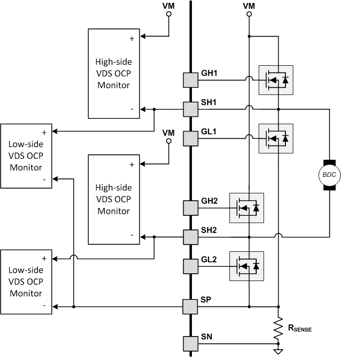 Figure 28. Overcurrent VDS Monitors
When IDRIVE is shorted to AVDD, the VDS OCP monitor on the high-side FETs is disabled. In cases where the VM supplied to the DRV8701 can be different from the external H-bridge supply, this setting must be used in order to prevent false overcurrent detection. In this mode, the IDRIVE current is set to 25-mA source and 50-mA sink.
7.3.10 Charge Pump
A charge pump is integrated to supply a high-side NMOS gate drive voltage of VHGS. The charge pump requires a capacitor between the VM and VCP pins. Additionally a low-ESR ceramic capacitor is required between pins CPH and CPL. When VM is below 12 V, this charge pump behaves as a doubler and generates VCP = 2 × VM – 1.5 V if unloaded. Above VM = 12 V, the charge pump regulates VCP such that VCP = VM + 9.5 V.
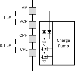 Figure 29. Charge Pump Diagram
7.3.11 LDO Voltage Regulators
Two LDO regulators are integrated into the DRV8701. They can be used to provide the supply voltage for a low-power microcontroller or other low-current devices. For proper operation, bypass the AVDD and DVDD pins to GND using ceramic capacitors.
The AVDD output voltage is nominally 4.8 V, and the DVDD output is nominally 3.3 V. When the AVDD or DVDD current load exceeds 30 mA, the LDO behaves like a constant current source. The output voltage drops significantly with currents greater than this limit.
Note that AVDD and DVDD are disabled when the device is in sleep mode (nSLEEP = 0). In addition, when an overtemperature (TSD) or undervoltage (UVLO) fault is encountered, the AVDD regulator is shut off.
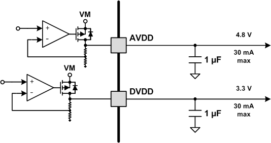 Figure 30. AVDD and DVDD LDOs
The power dissipated in the DRV8701 due to these LDOs may be approximated by:
For example at VM = 24 V, drawing 10 mA out of both AVDD and DVDD results in a power dissipation of:
7.3.12 Gate Drive Clamp
A clamping structure limits the gate drive output voltage to VGS CLAMP to protect the power FETs from damage. The positive voltage clamp is realized using a series of diodes. The negative voltage clamp uses the body diodes of the internal gate driver FET.
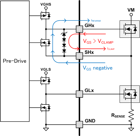 Figure 31. Gate Drive Clamp Diagram
7.3.13 Protection Circuits
The DRV8701 is fully protected against VM undervoltage, charge pump undervoltage, overcurrent, gate driver shorts, and overtemperature events.
7.3.13.1 VM Undervoltage Lockout (UVLO)
If at any time the voltage on the VM pin falls below the UVLO threshold voltage, all FETs in the H-bridge are disabled, the charge pump is disabled, AVDD is disabled, and the nFAULT pin is driven low. Operation resumes when VM rises above the UVLO threshold. The nFAULT pin is released after operation has resumed.
7.3.13.2 VCP Undervoltage Lockout (CPUV)
If at any time the voltage on the VCP pin falls below the charge pump undervoltage threshold voltage (VCPUV), all FETs in the H-bridge are disabled and the nFAULT pin is driven low. Operation resumes when VCP rises above the CPUV threshold. The nFAULT pin is released after operation has resumed.
7.3.13.3 Overcurrent Protection (OCP)
Overcurrent is sensed by monitoring the VDS voltage drop across the external FETs (see Figure 28). If the voltage across a driven FET exceeds the overcurrent trip threshold (VDS OCP) for longer than the OCP deglitch time (tOCP), an OCP event is recognized. As a result, all FETs in the H-bridge are disabled and the nFAULT pin is driven low; the driver is re-enabled after the OCP retry period (tRETRY) has passed. nFAULT releases high-Z again at after the retry time. If the fault condition is still present, the cycle repeats. If the fault is no longer present, normal operation resumes and nFAULT remains released high-Z.
This VDS overcurrent monitor on the high-side FETs can be disabled by using a specific IDRIVE setting. This allows the system to have a higher DRV8701 VM supply than the H-bridge supply.
In addition to this FET VDS monitor, an overcurrent condition is also detected if the voltage at SP exceeds
VSP OCP.
7.3.13.4 Pre-Driver Fault (PDF)
The GHx and GLx pins are monitored such that if the voltage on the external FET gate does not increase above 1 V (when sourcing current) or decrease below 1 V (when sinking current) after tDRIVE, a pre-driver fault is detected. The device encounters this fault if GHx or GLx are shorted to GND, SHx, or VM. Additionally, the device encounters the pre-driver fault if the IDRIVE setting selected is not sufficient to turn on the external FET. As a result, all FETs in the H-bridge are disabled and the nFAULT pin is driven low. The driver is re-enabled after the retry period (tRETRY) has passed. The nFAULT pin is released after operation has resumed.
7.3.13.5 Thermal Shutdown (TSD)
If the die temperature exceeds TTSD, all FETs in the H-bridge are disabled, the charge pump is shut down, AVDD is disabled, and the nFAULT pin is driven low. After the die temperature has fallen below TTSD – THYS, operation automatically resumes. The nFAULT pin is released after operation has resumed.
Table 7. Fault Response
| Fault | Condition | H-Bridge | Charge Pump | AVDD | DVDD | Recovery |
|---|---|---|---|---|---|---|
| VM undervoltage (UVLO) | VM ≤ VUVLO | Disabled | Disabled | Disabled | Operating | VM ≥ VUVLO |
| VCP undervoltage (CPUV) | VCP < VCPUV | Disabled | Operating | Operating | Operating | VCP > VCPUV |
| External FET overload (OCP) | VDS ≥ 1.0 V or VSP – VSN > 1.0 V |
Disabled | Operating | Operating | Operating | tRETRY |
| Pre-driver fault (PDF) | Gate voltage unchanged after tDRIVE | Disabled | Operating | Operating | Operating | tRETRY |
| Thermal shutdown (TSD) | TJ ≥ 150°C | Disabled | Disabled | Disabled | Operating | TJ ≤ 130°C |
7.3.14 Reverse Supply Protection
The following circuit may be implemented to protect the system from reverse supply conditions. This circuit requires the following additional components:
- NMOS FET
- npn BJT
- Diode
- 10-kΩ resistor
- 43-kΩ resistor
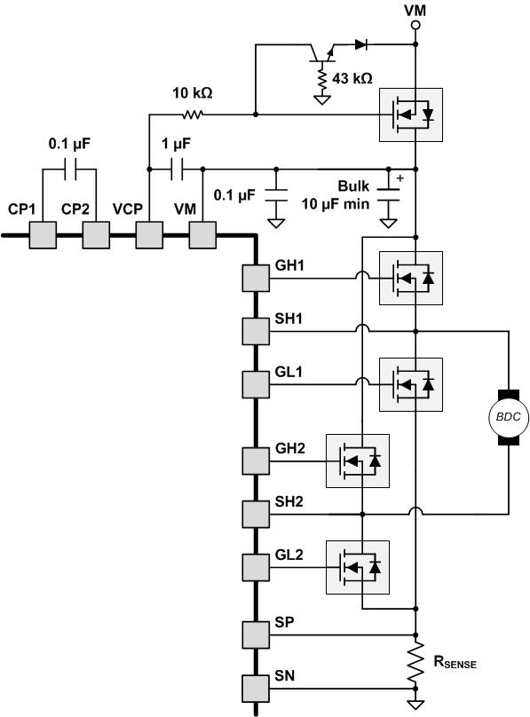 Figure 32. Reverse Supply Protection External Circuitry
7.4 Device Functional Modes
The DRV8701 is active unless the nSLEEP pin is brought low. In sleep mode, the charge pump is disabled, the H-bridge FETs are High-Z, and the AVDD and DVDD regulators are disabled. Note that tSLEEP must elapse after a falling edge on the nSLEEP pin before the device is in sleep mode. The DRV8701 is brought out of sleep mode if nSLEEP is brought high. Note that tWAKE must elapse before the outputs change state after wake-up.
While nSLEEP is brought low, all external H-bridge FETs are disabled. The high-side gate pins GHx are pulled to the output node SHx by an internal resistor, and the low-side gate pins GLx are pulled to GND.
When VM is not applied, and during the power-on time (tON), the outputs are disabled using weak pulldown resistors between the GHx and SHx pins and between GLx and GND.
Table 8. Functional Modes
| Condition | Charge Pump | GHx | GLx | AVDD and DVDD | |
|---|---|---|---|---|---|
| Unpowered | VM < VUVLO | Disabled | Weak pulldown to SHx | Weak pulldown to GND | Disabled |
| Sleep mode | VUVLO < VM nSLEEP low |
Disabled | Strong pulldown to GND | Strong pulldown to GND | Disabled |
| Operating | VUVLO < VM nSLEEP high |
Enabled | Depends on inputs | Depends on inputs | Operating |
7.4.1 Operating DRV8701 and H-Bridge on Separate Supplies
The DRV8701 can operate with a different supply voltage (VM) than the system H-bridge supply (VBAT). Case 1 describes normal operation when VM and VBAT are roughly the same. Special considerations must be taken into account for Cases 2, 3, and 4.
- Case 1: VM ≈ VBAT. Recommended operation
- Case 2: VM > VBAT. IDRIVE must be shorted to AVDD to disable the high-side OCP. The IDRIVE current is fixed at 25-mA source and 50-mA sink. This case can allow the driver to better enhance the external FETs for VBAT < 11.5 V, or operate down to a lower supply voltage below 5.9 V.
- Case 3: VM > VBAT (higher than Case 2). IDRIVE must be shorted to AVDD to disable the high-side OCP. This case can also allow the driver to better enhance the external FETs, or operate down to a lower supply voltage below 5.9 V. The IDRIVE current is fixed at 25-mA source and 50-mA sink. Excess gate drive current may be driven through the DRV8701 gate clamps causing additional power dissipation in the DRV8701.
- Case 4: VM < VBAT. The high-side FETs may not be in saturation. There may be a significant voltage drop across the high-side FET when driving current. This causes high power dissipation in the external FET. When operating in Case 4, the external FET threshold voltage must be greater than 2 V. Otherwise the DRV8701 will report a pre-driver fault whenever the FET is out of saturation.
Table 9. VM Operational Range based on VBAT
| VBAT Range | Case 3 | Case 2 | Case 1 | Case 4 |
|---|---|---|---|---|
| 1 V ≤ VBAT < 5.9 V | VM ≥ 0.5 × VBAT + 5.75 V VM ≤ 45 V |
VM ≥ 5.9 V VM < 0.5 × VBAT + 5.75 V |
N/A | N/A |
| 5.9 V ≤ VBAT < 6.4 V | VM > VBAT VM < 0.5 × VBAT + 5.75 V |
VM = VBAT | VM ≥ 5.9 V VM < VBAT |
|
| 6.4 V ≤ VBAT < 11.5 V | VM > 0.6 × VBAT + 2.5 V VM ≤ VBAT |
VM ≥ 5.9 V VM ≤ 0.6 × VBAT + 2.5 V |
||
| 11.5 V ≤ VBAT < 14 V | VM > VBAT VM ≤ 45 V |
N/A | ||
| 14 V ≤ VBAT ≤ 45 V | VM > VBAT – 4 V VM ≤ VBAT |
VM ≥ 5.9 V VM ≤ VBAT – 4 V |
 Figure 33. VM Operating Range Based on Motor Supply Voltage
When nSLEEP is low, VM may be reduced down to 0 V with up to 45 V present at VBAT. However, nSLEEP should not be brought high until VM is supplied with a voltage aligning with one of the cases outlined above.