SLLSFA7A July 2020 – April 2021 DRV8706-Q1
PRODUCTION DATA
- 1 Features
- 2 Applications
- 3 Descriptions
- 4 Revision History
- 5 Pin Configuration
- 6 Specifications
-
7 Detailed Description
- 7.1 Overview
- 7.2 Functional Block Diagram
- 7.3
Feature Description
- 7.3.1 External Components
- 7.3.2 Device Interface Variants
- 7.3.3 Input PWM Modes
- 7.3.4 Smart Gate Driver
- 7.3.5 Doubler (Single-Stage) Charge Pump
- 7.3.6 Wide Common Mode Differential Current Shunt Amplifier
- 7.3.7 Pin Diagrams
- 7.3.8
Protection and Diagnostics
- 7.3.8.1 Gate Driver Disable and Enable (DRVOFF and EN_DRV)
- 7.3.8.2 Fault Reset (CLR_FLT)
- 7.3.8.3 DVDD Logic Supply Power on Reset (DVDD_POR)
- 7.3.8.4 PVDD Supply Undervoltage Monitor (PVDD_UV)
- 7.3.8.5 PVDD Supply Overvoltage Monitor (PVDD_OV)
- 7.3.8.6 VCP Charge Pump Undervoltage Lockout (VCP_UV)
- 7.3.8.7 MOSFET VDS Overcurrent Protection (VDS_OCP)
- 7.3.8.8 Gate Driver Fault (VGS_GDF)
- 7.3.8.9 Thermal Warning (OTW)
- 7.3.8.10 Thermal Shutdown (OTSD)
- 7.3.8.11 Offline Short Circuit and Open Load Detection (OOL and OSC)
- 7.3.8.12 Fault Detection and Response Summary Table
- 7.4 Device Function Modes
- 7.5 Programming
- 7.6 Register Maps
- 8 Application and Implementation
- 9 Layout
- 10Device and Documentation Support
- 11Mechanical, Packaging, and Orderable Information
Package Options
Refer to the PDF data sheet for device specific package drawings
Mechanical Data (Package|Pins)
- RHB|32
Thermal pad, mechanical data (Package|Pins)
- RHB|32
Orderable Information
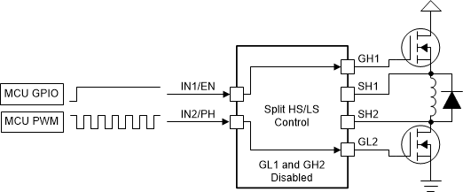
7.3.3.3 Split HS and LS Solenoid Control
In split HS and LS solenoid control mode, only the GH1 and GL2 gate driver outputs are active. The GH1 output is controlled through IN1/EN and the GL2 output is controlled through IN2/PH. This mode allows for the H-bridge to be configured to drive a floating solenoid load between the opposite high-side and low-side external MOSFETs.
In the split HS and LS control mode, the nHIZx pins and S_HIZx register functions are disabled. The nHIZx pins can be left disconnected or tied to GND. The H-bridge can be set to the Hi-Z state through the DRVOFF pin or the EN_DRV register setting on SPI devices.
| IN1/EN | IN2/PH | GH1 | GL1 | GH2 | GL2 | DESCRIPTION |
|---|---|---|---|---|---|---|
| 0 | X | L | Inactive | Inactive | X | Solenoid Disabled |
| 1 | X | H | Inactive | Inactive | X | Solenoid Enabled |
| X | 0 | X | Inactive | Inactive | L | Solenoid PWM Off |
| X | 1 | X | Inactive | Inactive | H | Solenoid PWM On |
 Figure 7-6 Split HS and LS PWM Control