SLLSFA7A July 2020 – April 2021 DRV8706-Q1
PRODUCTION DATA
- 1 Features
- 2 Applications
- 3 Descriptions
- 4 Revision History
- 5 Pin Configuration
- 6 Specifications
-
7 Detailed Description
- 7.1 Overview
- 7.2 Functional Block Diagram
- 7.3
Feature Description
- 7.3.1 External Components
- 7.3.2 Device Interface Variants
- 7.3.3 Input PWM Modes
- 7.3.4 Smart Gate Driver
- 7.3.5 Doubler (Single-Stage) Charge Pump
- 7.3.6 Wide Common Mode Differential Current Shunt Amplifier
- 7.3.7 Pin Diagrams
- 7.3.8
Protection and Diagnostics
- 7.3.8.1 Gate Driver Disable and Enable (DRVOFF and EN_DRV)
- 7.3.8.2 Fault Reset (CLR_FLT)
- 7.3.8.3 DVDD Logic Supply Power on Reset (DVDD_POR)
- 7.3.8.4 PVDD Supply Undervoltage Monitor (PVDD_UV)
- 7.3.8.5 PVDD Supply Overvoltage Monitor (PVDD_OV)
- 7.3.8.6 VCP Charge Pump Undervoltage Lockout (VCP_UV)
- 7.3.8.7 MOSFET VDS Overcurrent Protection (VDS_OCP)
- 7.3.8.8 Gate Driver Fault (VGS_GDF)
- 7.3.8.9 Thermal Warning (OTW)
- 7.3.8.10 Thermal Shutdown (OTSD)
- 7.3.8.11 Offline Short Circuit and Open Load Detection (OOL and OSC)
- 7.3.8.12 Fault Detection and Response Summary Table
- 7.4 Device Function Modes
- 7.5 Programming
- 7.6 Register Maps
- 8 Application and Implementation
- 9 Layout
- 10Device and Documentation Support
- 11Mechanical, Packaging, and Orderable Information
Package Options
Refer to the PDF data sheet for device specific package drawings
Mechanical Data (Package|Pins)
- RHB|32
Thermal pad, mechanical data (Package|Pins)
- RHB|32
Orderable Information
7.3.5 Doubler (Single-Stage) Charge Pump
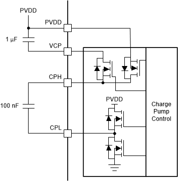
The high-side gate drive voltage for the external MOSFET is generated using a doubler charge pump that operates from the PVDD voltage supply input. The charge pump allows the high-side gate drivers to properly bias the external N-channel MOSFET with respect to its source voltage across a wide input supply voltage range. The charge pump output is regulated to maintain a fixed voltage respect to VPVDD and supports an average output current capability of 15-mA. The charge pump is continuously monitored for an undervoltage event to prevent under driven MOSFET conditions.
Since the charge pump is regulated to the PVDD pin voltage the device is not designed to support significant voltage differences between the PVDD and DRAIN pins and these should be limited.
The charge pumps requires a low ESR, 1-µF, 16-V ceramic capacitor (X5R or X7R recommended) between the PVDD and VCP pins to act as the storage capacitor. Additionally, a low ESR, 100-nF, PVDD-rated ceramic capacitor (X5R or X7R recommended) is required between the CPH and CPL pins to act as the flying capacitor.
 Figure 7-9 Charge Pump Architecture