SLVS855K July   2008  – March 2021 DRV8800 , DRV8801

PRODUCTION DATA  

  1. Features
  2. Applications
  3. Description
  4. Revision History
  5. Pin Configuration and Functions
  6. Specifications
    1. 6.1 Absolute Maximum Ratings
    2. 6.2 ESD Ratings
    3. 6.3 Recommended Operating Conditions
    4. 6.4 Thermal Information
    5. 6.5 Electrical Characteristics
    6. 6.6 Typical Characteristics
  7. Parameter Measurement Information
  8. Detailed Description
    1. 8.1 Overview
    2. 8.2 Functional Block Diagrams
    3. 8.3 Feature Description
      1. 8.3.1  Logic Inputs
      2. 8.3.2  VREG (DRV8800 Only)
      3. 8.3.3  VPROPI (DRV8801 Only)
        1. 8.3.3.1 Connecting VPROPI Output to ADC
      4. 8.3.4  Charge Pump
      5. 8.3.5  Shutdown
      6. 8.3.6  Low-Power Mode
      7. 8.3.7  Braking
      8. 8.3.8  Diagnostic Output
      9. 8.3.9  Thermal Shutdown (TSD)
      10. 8.3.10 Overcurrent Protection
      11. 8.3.11 SENSE
    4. 8.4 Device Functional Modes
      1. 8.4.1 Device Operation
        1. 8.4.1.1 Slow-Decay SR (Brake Mode)
        2. 8.4.1.2 Fast Decay With Synchronous Rectification
          1. 8.4.1.2.1 34
  9. Application and Implementation
    1. 9.1 Application Information
    2. 9.2 Typical Application
      1. 9.2.1 Design Requirements
      2. 9.2.2 Detailed Design Procedure
        1. 9.2.2.1 Motor Voltage
        2. 9.2.2.2 Power Dissipation
        3. 9.2.2.3 Thermal Considerations
          1. 9.2.2.3.1 Junction-to-Ambiant Thermal Impedance (ƟJA)
        4. 9.2.2.4 Motor Current Trip Point
        5. 9.2.2.5 Sense Resistor Selection
        6. 9.2.2.6 Drive Current
      3. 9.2.3 Pulse-Width Modulating
        1. 9.2.3.1 Pulse-Width Modulating ENABLE
        2. 9.2.3.2 Pulse-Width Modulating PHASE
      4. 9.2.4 Application Curves
    3. 9.3 Parallel Configuration
      1. 9.3.1 Parallel Connections
      2. 9.3.2 Non – Parallel Connections
      3. 9.3.3 Wiring nFAULT as Wired OR
      4. 9.3.4 Electrical Considerations
        1. 9.3.4.1 Device Spacing
        2. 9.3.4.2 Recirculation Current Handling
        3. 9.3.4.3 Sense Resistor Selection
        4. 9.3.4.4 Maximum System Current
  10. 10Power Supply Recommendations
    1. 10.1 Bulk Capacitance
  11. 11Layout
    1. 11.1 Layout Guidelines
    2. 11.2 Layout Example
  12. 12Device and Documentation Support
    1. 12.1 Related Links
    2. 12.2 Trademarks
    3. 12.3 Electrostatic Discharge Caution
    4. 12.4 Glossary
  13. 13Mechanical, Packaging, and Orderable Information

Package Options

Mechanical Data (Package|Pins)
Thermal pad, mechanical data (Package|Pins)
Orderable Information

Application Curves

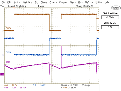
GUID-8AF1F72F-9965-4545-A0D7-F56628500FC5-low.pngFigure 9-3 Forward Drive, Fast Decay
GUID-04F2A388-3993-4CA2-93C4-2F0108170433-low.pngFigure 9-5 Forward Drive, Slow Decay
GUID-DEC0FD05-E373-4C56-9792-7C1B6BC87B8D-low.pngFigure 9-4 Reverse Drive, Fast Decay
GUID-F8EF7F55-5461-424C-9345-452E517EA418-low.pngFigure 9-6 Reverse Drive, Slow Decay