SLVSC79D June   2014  – November 2020 DRV8801A-Q1

PRODUCTION DATA  

  1. Features
  2. Applications
  3. Description
  4. Revision History
  5. Pin Configuration and Functions
  6. Specifications
    1. 6.1 Absolute Maximum Ratings
    2. 6.2 ESD Ratings
    3. 6.3 Recommended Operating Conditions
    4. 6.4 Thermal Information
    5. 6.5 Electrical Characteristics
    6. 6.6 Dissipation Ratings
    7. 6.7 Typical Characteristics
  7. Detailed Description
    1. 7.1 Overview
    2. 7.2 Functional Block Diagram
    3. 7.3 Feature Description
      1. 7.3.1 Power Supervisor
      2. 7.3.2 Bridge Control
        1. 7.3.2.1 MODE 1
        2. 7.3.2.2 MODE 2
      3. 7.3.3 Fast Decay with Synchronous Rectification
      4. 7.3.4 Slow Decay with Synchronous Rectification (Brake Mode)
      5. 7.3.5 Charge Pump
      6. 7.3.6 SENSE
      7. 7.3.7 VPROPI
        1. 7.3.7.1 Connecting VPROPI Output to ADC
      8. 7.3.8 Protection Circuits
        1. 7.3.8.1 VBB Undervoltage Lockout (UVLO)
        2. 7.3.8.2 Overcurrent Protection (OCP)
        3. 7.3.8.3 Overtemperature Warning (OTW)
        4. 7.3.8.4 Overtemperature Shutdown (OTS)
    4. 7.4 Device Functional Modes
  8. Application and Implementation
    1. 8.1 Application Information
    2. 8.2 Typical Application
      1. 8.2.1 Design Requirements
      2. 8.2.2 Detailed Design Procedure
        1. 8.2.2.1 Drive Current
        2. 8.2.2.2 40
        3. 8.2.2.3 Slow-Decay SR (Brake Mode)
      3. 8.2.3 Thermal Considerations
        1. 8.2.3.1 Junction-to-Ambiant Thermal Impedance (ƟJA)
      4. 8.2.4 Pulse-Width Modulating
        1. 8.2.4.1 Pulse-Width Modulating ENABLE
        2. 8.2.4.2 Pulse-Width Modulating PHASE
      5. 8.2.5 Application Curves
    3. 8.3 Parallel Configuration
      1. 8.3.1 Parallel Connections
      2. 8.3.2 Non – Parallel Connections
      3. 8.3.3 Wiring nFAULT as Wired OR
      4. 8.3.4 Electrical Considerations
        1. 8.3.4.1 Device Spacing
        2. 8.3.4.2 Recirculation Current Handling
        3. 8.3.4.3 Sense Resistor Selection
        4. 8.3.4.4 Maximum System Current
  9. Power Supply Recommendations
    1. 9.1 Bulk Capacitance
  10. 10Layout
    1. 10.1 Layout Guidelines
    2. 10.2 Layout Example
    3. 10.3 Power Dissipation
  11. 11Device and Documentation Support
    1. 11.1 Documentation Support
      1. 11.1.1 Related Documentation
    2. 11.2 Receiving Notification of Documentation Updates
    3. 11.3 Support Resources
    4. 11.4 Community Resources
    5. 11.5 Trademarks
    6. 11.6 Electrostatic Discharge Caution
    7. 11.7 Glossary
  12. 12Mechanical, Packaging, And Orderable Information

Package Options

Mechanical Data (Package|Pins)
Thermal pad, mechanical data (Package|Pins)
Orderable Information

Bulk Capacitance

Bulk capacitance sizing is an important factor in motor drive system design. This sizing is dependent on a variety of factors including:

  • Type of power supply
  • Acceptable supply voltage ripple
  • Parasitic inductance in the power supply wiring
  • Type of motor (brushed DC, brushless DC, stepper)
  • Motor startup current
  • Motor braking method

The inductance between the power supply and motor drive system will limit the rate current can change from the power supply. If the local bulk capacitance is too small, the system will respond to excessive current demands or dumps from the motor with a change in voltage. Size the bulk capacitance to meet acceptable voltage ripple levels.

The data sheet generally provides a recommended value but system-level testing is required to determine the appropriate sized bulk capacitor.
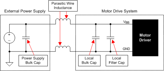
GUID-A69D773B-8826-4F4C-903D-C88CD987B460-low.gifFigure 9-1 Bulk Capacitance