DRV8802-Q1 Automotive DC Motor-Driver IC
1 Features
- Qualified for Automotive Applications
- AEC-Q100 Qualified With the Following Results
- Device Temperature Grade 1: –40°C to 125°C Ambient Operating Temperature
- Device HBM ESD Classification Level 2
- Device CDM ESD Classification Level C4B
- Dual H-Bridge Current-Control Motor Driver
- Drives Two DC Motors
- Brake Mode
- Two-Bit Winding Current Control Allows Up to 4 Current Levels
- Low MOSFET On-Resistance
- 1.6-A Maximum Drive Current at 24 V, 25°C
- Built-In 3.3-V Reference Output
- Industry Standard Parallel Digital Control
Interface - 8-V to 45-V Operating Supply Voltage Range
- Thermally Enhanced Surface Mount Package
2 Applications
- Automotive HVAC
- Automotive Valves
- Automotive Infotainment
3 Description
The DRV8802-Q1 device provides an integrated motor driver solution for automotive applications. The device has two H-bridge drivers, and is intended to drive DC motors. The output driver block for each consists of N-channel power MOSFET’s configured as H-bridges to drive the motor windings. The DRV8802-Q1 device can supply up to 1.6-A peak or 1.1-A RMS output current (with proper heatsinking at 24 V and 25°C) per H-bridge.
A simple parallel digital control interface is compatible with industry-standard devices. Decay mode is programmable to allow braking or coasting of the motor when disabled.
Internal shutdown functions are provided for over current protection, short circuit protection, under voltage lockout and overtemperature.
The DRV8802-Q1 device is available in a 28-pin HTSSOP package with PowerPAD™ (Eco-friendly: RoHS & no Sb/Br).
Device Information(1)
| PART NUMBER | PACKAGE | BODY SIZE (NOM) |
|---|---|---|
| DRV8802-Q1 | HTSSOP (28) | 9.70 mm × 4.40 mm |
- For all available packages, see the orderable addendum at the end of the datasheet.
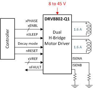
Simplified Application Diagram
4 Revision History
| DATE | REVISION | NOTES |
|---|---|---|
| June 2014 | A | Initial release. |
5 Pin Configuration and Functions

Pin Functions
| PIN | TYPE(1) | DESCRIPTION | EXTERNAL COMPONENTS OR CONNECTIONS |
|
|---|---|---|---|---|
| NAME | NO. | |||
| POWER AND GROUND | ||||
| CP1 | 1 | IO | Charge pump flying capacitor | Connect a 0.01-μF 50-V capacitor between CP1 and CP2. |
| CP2 | 2 | IO | Charge pump flying capacitor | |
| GND | 14 | — | Device ground | |
| 28 | ||||
| V3P3OUT | 15 | O | 3.3-V regulator output | Bypass to GND with a 0.47-μF 6.3-V ceramic capacitor. Can be used to supply VREF. |
| VMA | 4 | — | Bridge A power supply | Connect to motor supply (8 to 45 V). Both pins must be connected to same supply. |
| VMB | 11 | — | Bridge B power supply | |
| VCP | 3 | IO | High-side gate drive voltage | Connect a 0.1-μF 16-V ceramic capacitor and a 1-MΩ resistor to VMx. |
| CONTROL | ||||
| AI0 | 24 | I | Bridge A current set | Sets bridge A current: 00 = 100%, 01 = 71%, 10 = 38%, 11 = 0 |
| AI1 | 25 | I | ||
| AENBL | 21 | I | Bridge A enable | Logic high to enable bridge A |
| APHASE | 20 | I | Bridge A phase (direction) | Logic high sets AOUT1 high, AOUT2 low |
| AVREF | 12 | I | Bridge A current set reference input | Reference voltage for winding current set. Can be driven individually with an external DAC for microstepping, or tied to a reference (for example, V3P3OUT). |
| BVREF | 13 | I | Bridge B current set reference input | |
| BI0 | 26 | I | Bridge B current set | Sets bridge B current: 00 = 100%, 01 = 71%, 10 = 38%, 11 = 0 |
| BI1 | 27 | I | ||
| BENBL | 22 | I | Bridge B enable | Logic high to enable bridge B |
| BPHASE | 23 | I | Bridge B phase (direction) | Logic high sets BOUT1 high, BOUT2 low |
| DECAY | 19 | I | Decay (brake) mode | Low = brake (slow decay), high = coast (fast decay) |
| nRESET | 16 | I | Reset input | Active-low reset input initializes internal logic and disables the H-bridge outputs |
| nSLEEP | 17 | I | Sleep mode input | Logic high to enable device, logic low to enter low-power sleep mode |
| STATUS | ||||
| nFAULT | 18 | OD | Fault | Logic low when in fault condition (overtemperature, overcurrent) |
| OUTPUT | ||||
| AOUT1 | 5 | O | Bridge A output 1 | Connect to motor winding A |
| AOUT2 | 7 | O | Bridge A output 2 | |
| BOUT1 | 10 | O | Bridge B output 1 | Connect to motor winding B |
| BOUT2 | 8 | O | Bridge B output 2 | |
| ISENA | 6 | IO | Bridge A ground and current sense | Connect to current sense resistor for bridge A |
| ISENB | 9 | IO | Bridge B ground and current sense | Connect to current sense resistor for bridge B |
6 Specifications
6.1 Absolute Maximum Ratings
over operating free-air temperature range (unless otherwise noted)(1)(2)| MIN | MAX | UNIT | |||
|---|---|---|---|---|---|
| Power supply voltage | V(VMx) | –0.3 | 47 | V | |
| Charge pump voltage | VCP, CP1, CP2 | –0.3 | V(VMx)+7 | V | |
| Digital pin voltage | xPHASE, xENBL, nSLEEP, nFAULT, nRESET, xI0, xI1, DECAY | –0.5 | 7 | V | |
| Reference input voltage | V(xVREF) | –0.3 | 4 | V | |
| Sense pin voltage | V(ISENx) | –0.3 | 0.8 | V | |
| H-bridge output Current | xOUT1, xOUT2, ISENx | Peak motor drive, t < 1 μS | Internally limited | A | |
| Continuous motor drive(3) | 1.6 | A | |||
| Continuous total power dissipation | See the Power Dissipation section | ||||
| Operating virtual junction temperature, TJ | –40 | 150 | °C | ||
| Operating ambient temperature, TA | –40 | 125 | °C | ||
6.2 Handling Ratings
| MIN | MAX | UNIT | ||||
|---|---|---|---|---|---|---|
| Tstg | Storage temperature range | –60 | 150 | °C | ||
| V(ESD) | Electrostatic discharge | Human body model (HBM), per AEC Q100-002(1) | –2000 | 2000 | V | |
| Charged device model (CDM), per AEC Q100-011 | Corner pins (1, 14, 15, and 28) | –750 | 750 | |||
| Other pins | –500 | 500 | ||||
6.3 Recommended Operating Conditions
| MIN | MAX | UNIT | ||
|---|---|---|---|---|
| V(VMx) | Power supply voltage(1) | 8.2 | 45 | V |
| V(xVREF) | VREF input voltage(2) | 1 | 3.5 | V |
| I(OUT1x, OUT2x) | H-Bridge Output Current | 1.6 | A | |
| IL(V3P3OUT) | V3P3OUT load current | 1 | mA | |
6.4 Thermal Information
| THERMAL METRIC(1) | PWP | UNIT | |
|---|---|---|---|
| 28 PINS | |||
| RθJA | Junction-to-ambient thermal resistance | 38.9 | °C/W |
| RθJC(top) | Junction-to-case (top) thermal resistance | 23.3 | |
| RθJB | Junction-to-board thermal resistance | 21.2 | |
| ψJT | Junction-to-top characterization parameter | 0.8 | |
| ψJB | Junction-to-board characterization parameter | 20.9 | |
| RθJC(bot) | Junction-to-case (bottom) thermal resistance | 2.6 | |
6.5 Electrical Characteristics
over operating free-air temp range of -40°C to 125°C (unless otherwise noted)| PARAMETER | TEST CONDITIONS | MIN | TYP | MAX | UNIT | |
|---|---|---|---|---|---|---|
| POWER SUPPLIES | ||||||
| I(VMx) | VMx operating supply current | V(VMx) = 24 V, ƒ(PWM) < 50 kHz | 5 | 8 | mA | |
| I(VMx_Q) | VMx sleep mode supply current | V(VMx) = 24 V | 10 | 20 | μA | |
| V(UVLO) | VMx undervoltage lockout voltage | V(VMx) rising | 7.8 | 8.2 | V | |
| V3P3OUT REGULATOR | ||||||
| V(V3P3OUT) | V3P3OUT voltage | IO = 0 to 1 mA | 3.1 | 3.3 | 3.5 | V |
| LOGIC-LEVEL INPUTS | ||||||
| VIL | Input low voltage | 0.7 | V | |||
| VIH | Input high voltage | 2.1 | V | |||
| Vhys | Input hysteresis | 0.45 | V | |||
| IIL | Input low current | VI = 0 | –20 | 20 | μA | |
| IIH | Input high current | VI = 3.3 V | 100 | μA | ||
| nFAULT OUTPUT (OPEN-DRAIN OUTPUT) | ||||||
| VOL | Output low voltage | IO = 5 mA | 0.5 | V | ||
| IOH | Output high leakage current | VO = 3.3 V | 1 | μA | ||
| DECAY INPUT | ||||||
| VIL | Input low threshold voltage | For slow decay mode | 0 | 0.8 | V | |
| VIH | Input high threshold voltage | For fast decay mode | 2 | V | ||
| II | Input current | ±40 | µA | |||
| H-BRIDGE FETS | ||||||
| rDS(on) | HS FET on resistance | VM = 24 V, IO = 1 A, TJ = 25°C | 0.63 | Ω | ||
| VM = 24 V, IO = 1 A, TJ = 85°C | 0.76 | 0.9 | ||||
| VM = 24 V, IO = 1 A, TJ = 125°C | 0.85 | 1 | ||||
| rDS(on) | LS FET on resistance | VM = 24 V, IO = 1 A, TJ = 25°C | 0.65 | Ω | ||
| VM = 24 V, IO = 1 A, TJ = 85°C | 0.78 | 0.9 | ||||
| VM = 24 V, IO = 1 A, TJ = 125°C | 0.85 | 1 | ||||
| Ilkg(OFF) | Off-state leakage current | –20 | 20 | μA | ||
| MOTOR DRIVER | ||||||
| ƒ(PWM) | Internal PWM frequency | 50 | kHz | |||
| t(blank) | Current-sense blanking time | 3.75 | μs | |||
| tr | Rise time | VM = 24 V | 100 | 360 | ns | |
| tf | Fall time | VM = 24 V | 80 | 250 | ns | |
| t(dead) | Dead time | 400 | ns | |||
| PROTECTION CIRCUITS | ||||||
| I(OCP) | Overcurrent protection trip level | 1.8 | 5 | A | ||
| T(SD) | Thermal shutdown temperature | Die temperature | 150 | 160 | 180 | °C |
| CURRENT CONTROL | ||||||
| I(xVREF) | xVREF input current | V(xVREF) = 3.3 V | –3 | 3 | μA | |
| V(TRIP) | xISENSE trip voltage | V(xVREF) = 3.3 V, 100% current setting | 635 | 660 | 685 | mV |
| V(xVREF) = 3.3 V, 71% current setting | 445 | 469 | 492 | |||
| V(xVREF) = 3.3 V, 38% current setting | 225 | 251 | 276 | |||
| G(ISENx) | Current sense amplifier gain | Reference only | 5 | V/V | ||
6.6 Typical Characteristics


