SLVSAW4G July 2011 – December 2024 DRV8804
PRODUCTION DATA
- 1
- 1 Features
- 2 Applications
- 3 Description
- 4 Device Comparison
- 5 Pin Configuration and Functions
- 6 Specifications
- 7 Detailed Description
- 8 Application and Implementation
- 9 Device and Documentation Support
- 10Revision History
- 11Mechanical, Packaging, and Orderable Information
Package Options
Mechanical Data (Package|Pins)
Thermal pad, mechanical data (Package|Pins)
- PWP|16
Orderable Information
6.6 Timing Requirements
over operating free-air temperature range (unless otherwise noted)(1)
| MIN | NOM | MAX | UNIT | |||
|---|---|---|---|---|---|---|
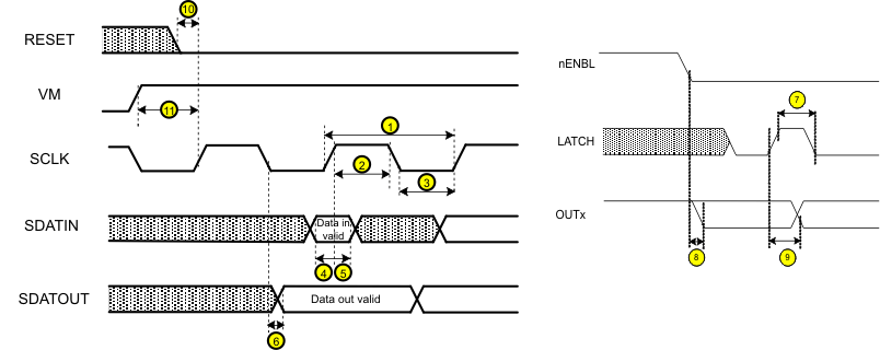
| 1 | tCYC | Clock cycle time | 62 | ns | ||
| 2 | tCLKH | Clock high time | 25 | ns | ||
| 3 | tCLKL | Clock low time | 25 | ns | ||
| 4 | tSU(SDATIN) | Setup time, SDATIN to SCLK | 5 | ns | ||
| 5 | tH(SDATIN) | Hold time, SDATIN to SCLK | 1 | ns | ||
| 6 | tD(SDATOUT) | Delay time, SCLK to SDATOUT, no external pullup resistor, COUT = 100 pF | 50 | 100 | ns | |
| 7 | tW(LATCH) | Pulse width, LATCH | 200 | ns | ||
| 8 | tOE(ENABLE) | Enable time, nENBL to output low | 60 | ns | ||
| 9 | tD(LATCH) | Delay time, LATCH to output change | 200 | ns | ||
| — | tRESET | RESET pulse width | 20 | µs | ||
| 10 | tD(RESET) | Reset delay before clock | 20 | µs | ||
| 11 | tSTARTUP | Start-up delay VM applied before clock | 55 | µs | ||
(1) Not production tested.

More than 400 ns of delay should exist between the final SCLK rising edge and the LATCH rising edge. This ensures that the last data bit is shifted into the device properly.
Figure 6-1 DRV8804 Timing Requirements