SLVSAW4G July 2011 – December 2024 DRV8804
PRODUCTION DATA
- 1
- 1 Features
- 2 Applications
- 3 Description
- 4 Device Comparison
- 5 Pin Configuration and Functions
- 6 Specifications
- 7 Detailed Description
- 8 Application and Implementation
- 9 Device and Documentation Support
- 10Revision History
- 11Mechanical, Packaging, and Orderable Information
Package Options
Mechanical Data (Package|Pins)
Thermal pad, mechanical data (Package|Pins)
- PWP|16
Orderable Information
7.3.2 Serial Interface Operation
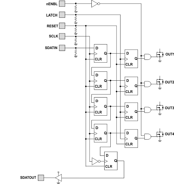
The DRV8804 is controlled with a simple serial interface. Logically, the interface is shown in Figure 7-1.
 Figure 7-1 Serial Interface Operation
Data is shifted into a temporary holding shift register in the part using the SDATIN pin, one bit at each rising edge of the SCLK pin. Data is simultaneously shifted out of the SDATOUT pin, allowing multiple devices to be daisy-chained onto one serial port. Note that the SDATOUT pin has a push-pull driver, which can support driving another DRV8804 SDATIN pin at clock frequencies of up to 1 MHz without an external pullup. A pullup resistor can be used between SDATOUT and an external 5-V logic supply to support higher clock frequencies. TI recommends a resistor value greater than 1 kΩ. The SDATOUT pin is capable of approximately 1-mA source and 5-mA sink. To supply logic signals to a lower-voltage microcontroller, use a resistor divider from SDATOUT to GND.
A rising edge on the LATCH pin latches the data from the temporary shift register into the output stage.