SLVSAW3D July 2011 – January 2016 DRV8805
PRODUCTION DATA.
- 1 Features
- 2 Applications
- 3 Description
- 4 Revision History
- 5 Pin Configuration and Functions
- 6 Specifications
- 7 Detailed Description
- 8 Application and Implementation
- 9 Power Supply Recommendations
- 10Layout
- 11Device and Documentation Support
- 12Mechanical, Packaging, and Orderable Information
Package Options
Mechanical Data (Package|Pins)
Thermal pad, mechanical data (Package|Pins)
- PWP|16
Orderable Information
5 Pin Configuration and Functions
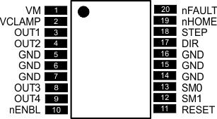
DW Package
20-Pin Wide SOIC
Top View

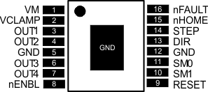
PWP Package
16-Pin HTSSOP
Top View

Pin Functions
| PIN | I/O(1) | DESCRIPTION | EXTERNAL COMPONENTS OR CONNECTIONS |
||
|---|---|---|---|---|---|
| NAME | SOIC | HTSSOP | |||
| POWER AND GROUND | |||||
| GND | 5, 6, 7, 14, 15, 16 |
5, 12, PPAD | — | Device ground | All pins must be connected to GND. |
| VM | 1 | 1 | — | Device power supply | Connect to motor supply (8.2 V to 60 V). |
| CONTROL | |||||
| DIR | 17 | 13 | I | Direction input | Level controls direction of rotation – internal pulldown |
| nENBL | 10 | 8 | I | Enable input | Active low enables outputs – internal pulldown |
| RESET | 11 | 9 | I | Reset input | Active-high reset input initializes internal logic – internal pulldown |
| SM0 | 13 | 11 | I | Step mode | Sets step mode – see step modes section for details – internal pulldowns |
| SM1 | 12 | 10 | |||
| STEP | 18 | 14 | I | Step input | Rising edge advances motor to next step – internal pulldown |
| STATUS | |||||
| nFAULT | 20 | 16 | OD | Fault | Logic low when in fault condition (overtemp, overcurrent) |
| nHOME | 19 | 15 | OD | Home | Logic low when indexer is at home position – push-pull structure |
| OUTPUT | |||||
| OUT1 | 3 | 3 | O | Output 1 | Connect to load 1 |
| OUT2 | 4 | 4 | O | Output 2 | Connect to load 2 |
| OUT3 | 8 | 6 | O | Output 3 | Connect to load 3 |
| OUT4 | 9 | 7 | O | Output 4 | Connect to load 4 |
| VCLAMP | 2 | 2 | — | Output clamp voltage | Connect to VM supply, or Zener diode to VM supply |
(1) Directions: I = input, O = output, OD = open-drain output