Refer to the PDF data sheet for device specific package drawings
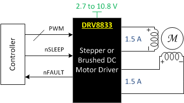
The DRV8833 device provides a dual bridge motor driver solution for toys, printers, and other mechatronic applications.
The device has two H-bridge drivers, and can drive two DC brush motors, a bipolar stepper motor, solenoids, or other inductive loads.
The output driver block of each H-bridge consists of N-channel power MOSFETs configured as an H-bridge to drive the motor windings. Each H-bridge includes circuitry to regulate or limit the winding current.
Internal shutdown functions with a fault output pin are provided for overcurrent protection, short-circuit protection, undervoltage lockout, and overtemperature. A low-power sleep mode is also provided.
The DRV8833 is packaged in a 16-pin WQFN package with PowerPAD™ (Eco-friendly: RoHS & no Sb/Br).
PART NUMBER | PACKAGE | BODY SIZE (NOM) |
---|---|---|
DRV8833 | TSSOP (16) | 5.00 mm × 4.40 mm |
HTSSOP (16) | 5.00 mm × 4.40 mm | |
WQFN (16) | 4.00 mm × 4.00 mm |
Changes from D Revision (March 2015) to E Revision
Changes from C Revision (January 2013) to D Revision
PIN | I/O(1) | DESCRIPTION | EXTERNAL COMPONENTS OR CONNECTIONS |
||
---|---|---|---|---|---|
NAME | WQFN | HTSSOP, TSSOP |
|||
POWER AND GROUND | |||||
GND | 11 PPAD |
13 | — | Device ground. HTSSOP package has PowerPAD. | Both the GND pin and device PowerPAD must be connected to ground. |
VINT | 12 | 14 | — | Internal supply bypass | Bypass to GND with 2.2-μF, 6.3-V capacitor. |
VM | 10 | 12 | — | Device power supply | Connect to motor supply. A 10-µF (minimum) ceramic bypass capacitor to GND is recommended. |
VCP | 9 | 11 | IO | High-side gate drive voltage | Connect a 0.01-μF, 16-V (minimum) X7R ceramic capacitor to VM. |
CONTROL | |||||
AIN1 | 14 | 16 | I | Bridge A input 1 | Logic input controls state of AOUT1. Internal pulldown. |
AIN2 | 13 | 15 | I | Bridge A input 2 | Logic input controls state of AOUT2. Internal pulldown. |
BIN1 | 7 | 9 | I | Bridge B input 1 | Logic input controls state of BOUT1. Internal pulldown. |
BIN2 | 8 | 10 | I | Bridge B input 2 | Logic input controls state of BOUT2. Internal pulldown. |
nSLEEP | 15 | 1 | I | Sleep mode input | Logic high to enable device, logic low to enter low-power sleep mode and reset all internal logic. Internal pulldown. |
STATUS | |||||
nFAULT | 6 | 8 | OD | Fault output | Logic low when in fault condition (overtemperature, overcurrent) |
OUTPUT | |||||
AISEN | 1 | 3 | IO | Bridge A ground / ISENSE | Connect to current sense resistor for bridge A, or GND if current control not needed |
BISEN | 4 | 6 | IO | Bridge B ground / ISENSE | Connect to current sense resistor for bridge B, or GND if current control not needed |
AOUT1 | 16 | 2 | O | Bridge A output 1 | Connect to motor winding A |
AOUT2 | 2 | 4 | O | Bridge A output 2 | |
BOUT1 | 5 | 7 | O | Bridge B output 1 | Connect to motor winding B |
BOUT2 | 3 | 5 | O | Bridge B output 2 |
MIN | MAX | UNIT | ||
---|---|---|---|---|
VM | Power supply voltage | –0.3 | 11.8 | V |
Digital input pin voltage | –0.5 | 7 | V | |
xISEN pin voltage | –0.3 | 0.5 | V | |
Peak motor drive output current | Internally limited | A | ||
TJ | Operating junction temperature | –40 | 150 | °C |
Tstg | Storage temperature | –60 | 150 | °C |
VALUE | UNIT | ||||
---|---|---|---|---|---|
V(ESD) | Electrostatic discharge | Human body model (HBM), per ANSI/ESDA/JEDEC JS-001, all pins(1) | ±4000 | V | |
Charged device model (CDM), per JEDEC specification JESD22-C101, all pins(2) | ±1500 |
MIN | NOM | MAX | UNIT | ||
---|---|---|---|---|---|
VM | Motor power supply voltage range(1) | 2.7 | 10.8 | V | |
VDIGIN | Digital input pin voltage range | –0.3 | 5.75 | V | |
IOUT | RTY package continuous RMS or DC output current per bridge(2) | 1.5 | A |
THERMAL METRIC(1) | DRV8833 | UNIT | |||
---|---|---|---|---|---|
PWP (HTSSOP) |
RTY (WQFN) |
PW (TSSOP) |
|||
16 PINS | 16 PINS | 16 PINS | |||
RθJA | Junction-to-ambient thermal resistance | 40.5 | 37.2 | 103.1 | °C/W |
RθJC(top) | Junction-to-case (top) thermal resistance | 32.9 | 34.3 | 38 | °C/W |
RθJB | Junction-to-board thermal resistance | 28.8 | 15.3 | 48.1 | °C/W |
ψJT | Junction-to-top characterization parameter | 0.6 | 0.3 | 3 | °C/W |
ψJB | Junction-to-board characterization parameter | 11.5 | 15.4 | 47.5 | °C/W |
RθJC(bot) | Junction-to-case (bottom) thermal resistance | 4.8 | 3.5 | N/A | °C/W |
PARAMETER | TEST CONDITIONS | MIN | TYP | MAX | UNIT | |
---|---|---|---|---|---|---|
POWER SUPPLY | ||||||
IVM | VM operating supply current | VM = 5 V, xIN1 = 0 V, xIN2 = 0 V | 1.7 | 3 | mA | |
IVMQ | VM sleep mode supply current | VM = 5 V | 1.6 | 2.5 | μA | |
VUVLO | VM undervoltage lockout voltage | VM falling | 2.6 | V | ||
VHYS | VM undervoltage lockout hysteresis | 90 | mV | |||
LOGIC-LEVEL INPUTS | ||||||
VIL | Input low voltage | nSLEEP | 0.5 | V | ||
All other pins | 0.7 | |||||
VIH | Input high voltage | nSLEEP | 2.5 | V | ||
All other pins | 2 | |||||
VHYS | Input hysteresis | 0.4 | V | |||
RPD | Input pulldown resistance | nSLEEP | 500 | kΩ | ||
All except nSLEEP | 150 | |||||
IIL | Input low current | VIN = 0 | 1 | μA | ||
IIH | Input high current | VIN = 3.3 V, nSLEEP | 6.6 | 13 | μA | |
VIN = 3.3 V, all except nSLEEP | 16.5 | 33 | ||||
tDEG | Input deglitch time | 450 | ns | |||
nFAULT OUTPUT (OPEN-DRAIN OUTPUT) | ||||||
VOL | Output low voltage | IO = 5 mA | 0.5 | V | ||
IOH | Output high leakage current | VO = 3.3 V | 1 | μA | ||
H-BRIDGE FETs | ||||||
RDS(ON) | HS FET on resistance | VM = 5 V, IO = 500 mA, TJ = 25°C | 200 | mΩ | ||
VM = 5 V, IO = 500 mA, TJ = 85°C | 325 | |||||
VM = 2.7 V, IO = 500 mA, TJ = 25°C | 250 | |||||
VM = 2.7 V, IO = 500 mA, TJ = 85°C | 350 | |||||
LS FET on resistance | VM = 5 V, IO = 500 mA, TJ = 25°C | 160 | ||||
VM = 5 V, IO = 500 mA, TJ = 85°C | 275 | |||||
VM = 2.7 V, IO = 500 mA, TJ = 25°C | 200 | |||||
VM = 2.7 V, IO = 500 mA, TJ = 85°C | 300 | |||||
IOFF | Off-state leakage current | VM = 5 V, TJ = 25°C, VOUT = 0 V | –1 | 1 | μA | |
MOTOR DRIVER | ||||||
ƒPWM | Current control PWM frequency | Internal PWM frequency | 50 | kHz | ||
tR | Rise time | VM = 5 V, 16 Ω to GND, 10% to 90% VM | 180 | ns | ||
tF | Fall time | VM = 5 V, 16 Ω to GND, 10% to 90% VM | 160 | ns | ||
tPROP | Propagation delay INx to OUTx | VM = 5 V | 1.1 | µs | ||
tDEAD | Dead time(1) | VM = 5 V | 450 | ns | ||
PROTECTION CIRCUITS | ||||||
IOCP | Overcurrent protection trip level | 2 | 3.3 | A | ||
tDEG | OCP Deglitch time | 4 | µs | |||
tOCP | Overcurrent protection period | 1.35 | ms | |||
tTSD | Thermal shutdown temperature | Die temperature | 150 | 160 | 180 | °C |
CURRENT CONTROL | ||||||
VTRIP | xISEN trip voltage | 160 | 200 | 240 | mV | |
tBLANK | Current sense blanking time | 3.75 | µs | |||
SLEEP MODE | ||||||
tWAKE | Start-up time | nSLEEP inactive high to H-bridge on | 1 | ms |
The DRV8833 device is an integrated motor driver solution for brushed DC or bipolar stepper motors. The device integrates two NMOS H-bridges and current regulation circuitry. The DRV8833 can be powered with a supply voltage from 2.7 to 10.8 V and can provide an output current up to 1.5-A RMS.
A simple PWM interface allows easy interfacing to the controller circuit.
The current regulation is a fixed frequency PWM slow decay.
The device includes a low-power sleep mode, which lets the system save power when not driving the motor.
DRV8833 contains two identical H-bridge motor drivers with current-control PWM circuitry. Figure 5 shows a block diagram of the circuitry.
The AIN1 and AIN2 input pins control the state of the AOUT1 and AOUT2 outputs; similarly, the BIN1 and BIN2 input pins control the state of the BOUT1 and BOUT2 outputs. Table 1 shows the logic.
xIN1 | xIN2 | xOUT1 | xOUT2 | FUNCTION |
---|---|---|---|---|
0 | 0 | Z | Z | Coast/fast decay |
0 | 1 | L | H | Reverse |
1 | 0 | H | L | Forward |
1 | 1 | L | L | Brake/slow decay |
The inputs can also be used for PWM control of the motor speed. When controlling a winding with PWM, when the drive current is interrupted, the inductive nature of the motor requires that the current must continue to flow. This is called recirculation current. To handle this recirculation current, the H-bridge can operate in two different states: fast decay or slow decay. In fast decay mode, the H-bridge is disabled and recirculation current flows through the body diodes; in slow decay, the motor winding is shorted.
To PWM using fast decay, the PWM signal is applied to one xIN pin while the other is held low; to use slow decay, one xIN pin is held high.
xIN1 | xIN2 | FUNCTION |
---|---|---|
PWM | 0 | Forward PWM, fast decay |
1 | PWM | Forward PWM, slow decay |
0 | PWM | Reverse PWM, fast decay |
PWM | 1 | Reverse PWM, slow decay |
Figure 6 shows the current paths in different drive and decay modes.
The current through the motor windings may be limited, or controlled, by a fixed-frequency PWM current regulation, or current chopping. For DC motors, current control is used to limit the start-up and stall current of the motor. For stepper motors, current control is often used at all times.
When an H-bridge is enabled, current rises through the winding at a rate dependent on the DC voltage and inductance of the winding. If the current reaches the current chopping threshold, the bridge disables the current until the beginning of the next PWM cycle. Immediately after the current is enabled, the voltage on the xISEN pin is ignored for a fixed period of time before enabling the current sense circuitry. This blanking time is fixed at 3.75 μs. This blanking time also sets the minimum on time of the PWM when operating in current chopping mode.
The PWM chopping current is set by a comparator which compares the voltage across a current sense resistor connected to the xISEN pins with a reference voltage. The reference voltage is fixed at 200 mV.
The chopping current is calculated in Equation 1.
Example: If a 1-Ω sense resistor is used, the chopping current will be 200 mV/1 Ω = 200 mA.
Once the chopping current threshold is reached, the H-bridge switches to slow decay mode. Winding current is recirculated by enabling both of the low-side FETs in the bridge. This state is held until the beginning of the next fixed-frequency PWM cycle.
If current control is not needed, the xISEN pins should be connected directly to ground.
Driving nSLEEP low will put the device into a low power sleep state. In this state, the H-bridges are disabled, the gate drive charge pump is stopped, all internal logic is reset, and all internal clocks are stopped. All inputs are ignored until nSLEEP returns inactive high. When returning from sleep mode, some time (up to 1 ms) needs to pass before the motor driver becomes fully operational. To make the board design simple, the nSLEEP can be pulled up to the supply (VM). TI recommends using a pullup resistor when this is done. This resistor limits the current to the input in case VM is higher than 6.5 V. Internally, the nSLEEP pin has a 500-kΩ resistor to GND. It also has a clamping Zener diode that clamps the voltage at the pin at 6.5 V. Currents greater than 250 µA can cause damage to the input structure. Hence the recommended pullup resistor would be between 20 kΩ and
75 kΩ.
The DRV8833 is fully protected against undervoltage, overcurrent and overtemperature events.
An analog current limit circuit on each FET limits the current through the FET by limiting the gate drive. If this analog current limit persists for longer than the OCP deglitch time, all FETs in the H-bridge will be disabled and the nFAULT pin will be driven low. The driver will be re-enabled after the OCP retry period (tOCP) has passed. nFAULT becomes high again at this time. If the fault condition is still present, the cycle repeats. If the fault is no longer present, normal operation resumes and nFAULT remains deasserted. Please note that only the H-bridge in which the OCP is detected will be disabled while the other bridge will function normally.
Overcurrent conditions are detected independently on both high- and low-side devices; that is, a short to ground, supply, or across the motor winding will all result in an overcurrent shutdown. Overcurrent protection does not use the current sense circuitry used for PWM current control, so it functions even without presence of the xISEN resistors.
If the die temperature exceeds safe limits, all FETs in the H-bridge will be disabled and the nFAULT pin will be driven low. Once the die temperature has fallen to a safe level, operation will automatically resume.
If at any time the voltage on the VM pin falls below the undervoltage lockout threshold voltage, all circuitry in the device will be disabled, and all internal logic will be reset. Operation will resume when VM rises above the UVLO threshold. nFAULT is driven low in the event of an undervoltage condition.
FAULT | CONDITION | ERROR REPORT | H-BRIDGE | INTERNAL CIRCUITS | RECOVERY |
---|---|---|---|---|---|
VM undervoltage (UVLO) | VM < 2.5 V | None | Disabled | Disabled | VM > 2.7 V |
Overcurrent (OCP) | IOUT > IOCP | FAULTn | Disabled | Operating | OCP |
Thermal Shutdown (TSD) | TJ > TTSD | FAULTn | Disabled | Operating | TJ < TTSD – THYS |
The DRV8833 is active unless the nSLEEP pin is brought logic low. In sleep mode, the H-bridge FETs are disabled (Hi-Z). The DRV8833 is brought out of sleep mode automatically if nSLEEP is brought logic high. tWAKE must elapse before the outputs change state after wakeup.
FAULT | CONDITION | H-BRIDGE | INTERNAL CIRCUITS |
---|---|---|---|
Operating | nSLEEP pin high | Operating | Operating |
Sleep mode | nSLEEP pin low | Disabled | Disabled |
Fault encountered | Any fault condition met | Disabled | See Table 3 |