SLVSBA2D July 2012 – May 2016 DRV8844
PRODUCTION DATA.
- 1 Features
- 2 Applications
- 3 Description
- 4 Revision History
- 5 Pin Configuration and Functions
- 6 Specifications
- 7 Detailed Description
- 8 Application and Implementation
- 9 Power Supply Recommendations
- 10Layout
- 11Device and Documentation Support
- 12Mechanical, Packaging, and Orderable Information
Package Options
Mechanical Data (Package|Pins)
- PWP|28
Thermal pad, mechanical data (Package|Pins)
- PWP|28
Orderable Information
8 Application and Implementation
NOTE
Information in the following applications sections is not part of the TI component specification, and TI does not warrant its accuracy or completeness. TI’s customers are responsible for determining suitability of components for their purposes. Customers should validate and test their design implementation to confirm system functionality.
8.1 Application Information
The DRV8844 can be used to drive one stepper motor, multiple brushed DC motors, or multiple other inductive loads.
The outputs can be connected in parallel to increase the drive current. If connecting the outputs as in a full-bridge configuration, any two outputs can be connected in parallel. If configured as two independent half bridges, OUT1 and OUT2 must be paired, and OUT3 and OUT4 must be paired. This pairing is because pin 6 (SRC12) is the source for the low-side FETs of OUT1 and OUT2, and pin 9 (SRC34) is the source for the low-side FETs of OUT3 and OUT4.
An optional sense resistor can be used to monitor the current. If using sense resistors, place the resistor between the SRC12 or SRC34 pins and the VNEG pins.
8.2 Typical Application
 Figure 8. Stepper Motor Connections
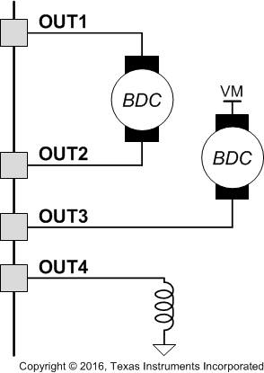
 Figure 9. Example Showing a Bidirectional Brushed DC Motor,
 Single-Direction Brushed DC Motor, and an Inductive Load
8.2.1 Design Requirements
The following truth tables describe how to control the arrangement in Figure 8.
Table 3. Brushed DC Motor
| FUNCTION | EN1 | EN2 | IN1 | IN2 | OUT1 | OUT2 |
|---|---|---|---|---|---|---|
| Forward | 1 | 1 | PWM | 0 | H | L |
| Reverse | 1 | 1 | 0 | PWM | L | H |
| Brake | 1 | 1 | 0 | 0 | L | L |
| Brake | 1 | 1 | 1 | 1 | H | H |
| Coast | 0 | X | X | X | Z | X |
| Coast | X | 0 | X | X | X | Z |
Table 4. Single-Direction Brushed DC Motor
| FUNCTION | EN3 | IN3 | OUT3 |
|---|---|---|---|
| On | 1 | PWM | L |
| Brake | 1 | 1 | H |
| Coast | 0 | X | Z |
Table 5. Inductive Loads
| FUNCTION | EN4 | IN4 | OUT4 |
|---|---|---|---|
| On | 1 | PWM | H |
| Off or slow decay | 1 | 0 | L |
| Off or coast | 0 | X | Z |
8.2.2 Detailed Design Procedure
8.2.2.1 Motor Voltage
The ratings of the motor selected and the desired RPM determine the motor voltage the designer should use. A higher voltage spins a brushed DC motor faster with the same PWM duty cycle applied to the power FETs. A higher voltage also increases the rate of current change through the inductive motor windings.
8.2.3 Application Curves
 Figure 10. DC Motor With 80 PWM
 Figure 11. IN1 to OUT1 Propagation Delay