SLVSE65C July 2018 – December 2023 DRV8847
PRODUCTION DATA
- 1
- 1 Features
- 2 Applications
- 3 Description
- 4 Revision History
- 5 Pin Configuration and Functions
- 6 Specifications
-
7 Detailed Description
- 7.1 Overview
- 7.2 Functional Block Diagram
- 7.3
Feature Description
- 7.3.1 PWM Motor Drivers
- 7.3.2 Bridge Operation
- 7.3.3 Bridge Control
- 7.3.4 Current Regulation
- 7.3.5 Current Recirculation and Decay Modes
- 7.3.6 Torque Scalar
- 7.3.7 Stepping Modes
- 7.3.8 Motor Driver Protection Circuits
- 7.4 Device Functional Modes
- 7.5 Programming
- 7.6
Register Map
- 7.6.1 Slave Address Register (Address = 0x00) [reset = 0x60]
- 7.6.2 IC1 Control Register (Address = 0x01) [reset = 0x00]
- 7.6.3 IC2 Control Register (Address = 0x02) [reset = 0x00]
- 7.6.4 Slew-Rate and Fault Status-1 Register (Address = 0x03) [reset = 0x40]
- 7.6.5 Fault Status-2 Register (Address = 0x04) [reset = 0x00]
-
8 Application and Implementation
- 8.1 Application Information
- 8.2
Typical Application
- 8.2.1 Stepper Motor Application
- 8.2.2 Dual BDC Motor Application
- 8.2.3 Open Load Implementation
- Power Supply Recommendations
- 9 Layout
- 10Device and Documentation Support
- 11Mechanical, Packaging, and Orderable Information
Package Options
Refer to the PDF data sheet for device specific package drawings
Mechanical Data (Package|Pins)
- PW|16
- PWP|16
- RTE|16
Thermal pad, mechanical data (Package|Pins)
- RTE|16
Orderable Information
7.3.8.4.1 Full-Bridge Open Load Detection
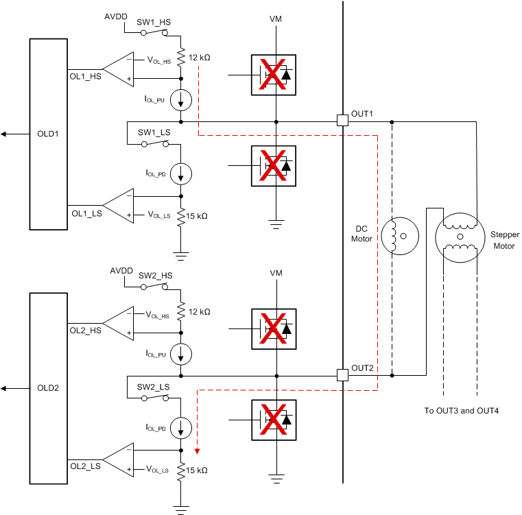
As shown in Figure 7-20, during device wakeup, a constant current source pulls the OUT1 pin to the AVDD (internal) fixed voltage which allows current flow from OUT1 to OUT2 terminal. The current drawn is completely dependent on the motor resistance between OUT1 and OUT2. Depending on this current and the comparator threshold voltage (VOL_HS and VOL_LS), the comparator output OL1_HS and OL2_LS are either set or reset which determines the open load status. Table 7-9 shows the states of OL1_HS and OL2_LS for the open load detect. This test executes before the tWAKE or tON time has elapsed. When an open load is detected, the nFAULT pin is latched low until the device is power cycled or device reset with nSLEEP pin. A similar implementation is done for the OUT3 and OUT4 pins.
| OL1_HS | OL2_LS | OLD STATUS |
|---|---|---|
| 0 | 0 | NO OLD |
| 0 | 1 | |
| 1 | 0 | |
| 1 | 1 | OLD |
 Figure 7-20 Open Load Detect Circuit for Full-Bridge Connection
AVDD voltage is the internal regulator voltage and is determined as min (VVM, 4.2 V). Hence, for supply voltage (VVM) higher than 4.2 V, this voltage is fixed at 4.2 V else it is equal to supply voltage ( VVM).