SLRS065E September   2013  – November 2015 DRV8860

PRODUCTION DATA.  

  1. Features
  2. Applications
  3. Description
  4. Simplified Schematic
  5. Revision History
  6. Pin Configuration and Functions
  7. Specifications
    1. 7.1 Absolute Maximum Ratings
    2. 7.2 Handling Ratings
    3. 7.3 Recommended Operating Conditions
    4. 7.4 Thermal Information
    5. 7.5 Electrical Characteristics
    6. 7.6 Timing Requirements
    7. 7.7 Typical Characteristics
  8. Detailed Description
    1. 8.1 Overview
    2. 8.2 Functional Block Diagram
    3. 8.3 Feature Description
      1. 8.3.1 Recommended Output Current
      2. 8.3.2 Daisy Chain Connection
      3. 8.3.3 Protection Circuits
        1. 8.3.3.1 Overcurrent Protection (OCP)
        2. 8.3.3.2 Open Load Detection (OL) - DRV8860 only
        3. 8.3.3.3 Thermal Shutdown (TSD)
        4. 8.3.3.4 Undervoltage Lockout (UVLO)
        5. 8.3.3.5 Digital Noise Filter
    4. 8.4 Device Functional Modes
      1. 8.4.1 Internal Registers
    5. 8.5 Programming
      1. 8.5.1 Serial Control Interface
        1. 8.5.1.1 Data Writing Waveform
        2. 8.5.1.2 Fault Register Reading Waveform
        3. 8.5.1.3 Special Command
          1. 8.5.1.3.1 Special command: Write Control Register
          2. 8.5.1.3.2 Special command: Read Control Register
          3. 8.5.1.3.3 Special command: Read Data Register
          4. 8.5.1.3.4 Special command: Fault Register Reset
          5. 8.5.1.3.5 Special command: PWM Start
        4. 8.5.1.4 Output Energizing and PWM Control
          1. 8.5.1.4.1 PWM Start Special Command Used
    6. 8.6 Register Maps
      1. 8.6.1 Data Register
      2. 8.6.2 Fault Register
      3. 8.6.3 Control Register
  9. Application and Implementation
    1. 9.1 Application Information
    2. 9.2 Typical Application
      1. 9.2.1 Design Requirements
      2. 9.2.2 Detailed Design Procedure
        1. 9.2.2.1 Drive Current
      3. 9.2.3 Application Curves
  10. 10Power Supply Recommendations
    1. 10.1 Power Supply and Logic Sequencing
  11. 11Layout
    1. 11.1 Layout Guidelines
    2. 11.2 Layout Example
    3. 11.3 Thermal Consideration
      1. 11.3.1 Power Dissipation
      2. 11.3.2 Heatsinking
  12. 12Device and Documentation Support
    1. 12.1 Community Resources
    2. 12.2 Trademarks
    3. 12.3 Electrostatic Discharge Caution
    4. 12.4 Glossary
  13. 13Mechanical, Packaging, and Orderable Information

Package Options

Mechanical Data (Package|Pins)
Thermal pad, mechanical data (Package|Pins)
Orderable Information

9 Application and Implementation

NOTE

Information in the following applications sections is not part of the TI component specification, and TI does not warrant its accuracy or completeness. TI’s customers are responsible for determining suitability of components for their purposes. Customers should validate and test their design implementation to confirm system functionality.

9.1 Application Information

The DRV8860 is an eight channel low side driver with protection features. The following design is a common application of the DRV8860.

9.2 Typical Application
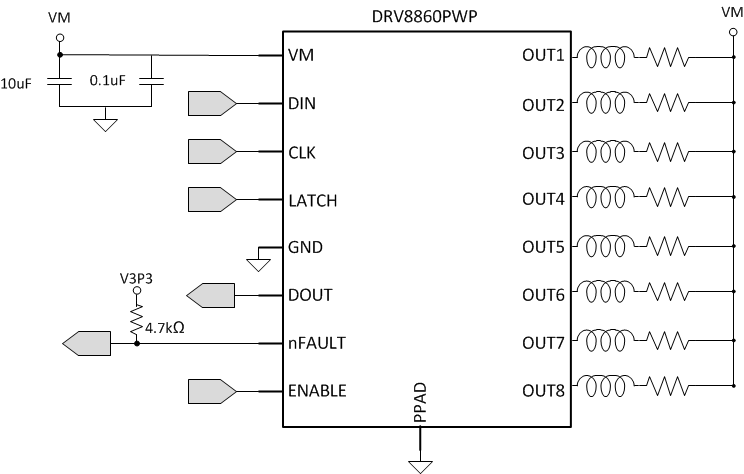
DRV8860 DRV8860A Application_circuit_slrs065.gif

9.2.1 Design Requirements

Table 5. Design Parameters

Parameter Value
Input voltage range 8 V – 38 V
Current 330 mA per channel

9.2.2 Detailed Design Procedure

9.2.2.1 Drive Current

The current path is from VM, through the load, into the low-side sinking driver. Power dissipation I2R losses in one sink are calculated using Equation 1.

Equation 1. PD = I2 x RDS(on)

9.2.3 Application Curves

DRV8860 DRV8860A PWM_Operation_Scope_slrs065.png Figure 37. PWM Operation