SLVSCY9B August   2015  – July 2016 DRV8871

PRODUCTION DATA.  

  1. Features
  2. Applications
  3. Description
    1.     Device Images
      1.      Simplified Schematic
      2.      Peak Current Regulation
  4. Revision History
  5. Pin Configuration and Functions
    1.     Pin Functions
  6. Specifications
    1. 6.1 Absolute Maximum Ratings
    2. 6.2 ESD Ratings
    3. 6.3 Recommended Operating Conditions
    4. 6.4 Thermal Information
    5. 6.5 Electrical Characteristics
    6. 6.6 Typical Characteristics
  7. Detailed Description
    1. 7.1 Overview
    2. 7.2 Functional Block Diagram
    3. 7.3 Feature Description
      1. 7.3.1 Bridge Control
      2. 7.3.2 Sleep Mode
      3. 7.3.3 Current Regulation
      4. 7.3.4 Dead Time
      5. 7.3.5 Protection Circuits
        1. 7.3.5.1 VM Undervoltage Lockout (UVLO)
        2. 7.3.5.2 Overcurrent Protection (OCP)
        3. 7.3.5.3 Thermal Shutdown (TSD)
    4. 7.4 Device Functional Modes
      1. 7.4.1 PWM With Current Regulation
      2. 7.4.2 PWM Without Current Regulation
      3. 7.4.3 Static Inputs With Current Regulation
      4. 7.4.4 VM Control
  8. Application and Implementation
    1. 8.1 Application Information
    2. 8.2 Typical Application
      1. 8.2.1 Design Requirements
      2. 8.2.2 Detailed Design Procedure
        1. 8.2.2.1 Motor Voltage
        2. 8.2.2.2 Drive Current
      3. 8.2.3 Application Curves
  9. Power Supply Recommendations
    1. 9.1 Bulk Capacitance
  10. 10Layout
    1. 10.1 Layout Guidelines
    2. 10.2 Layout Example
    3. 10.3 Thermal Considerations
    4. 10.4 Power Dissipation
      1. 10.4.1 Heatsinking
  11. 11Device and Documentation Support
    1. 11.1 Documentation Support
      1. 11.1.1 Related Documentation
    2. 11.2 Receiving Notification of Documentation Updates
    3. 11.3 Community Resources
    4. 11.4 Trademarks
    5. 11.5 Electrostatic Discharge Caution
    6. 11.6 Glossary
  12. 12Mechanical, Packaging, and Orderable Information

Package Options

Refer to the PDF data sheet for device specific package drawings

Mechanical Data (Package|Pins)
  • DDA|8
Thermal pad, mechanical data (Package|Pins)
Orderable Information

Application Curves

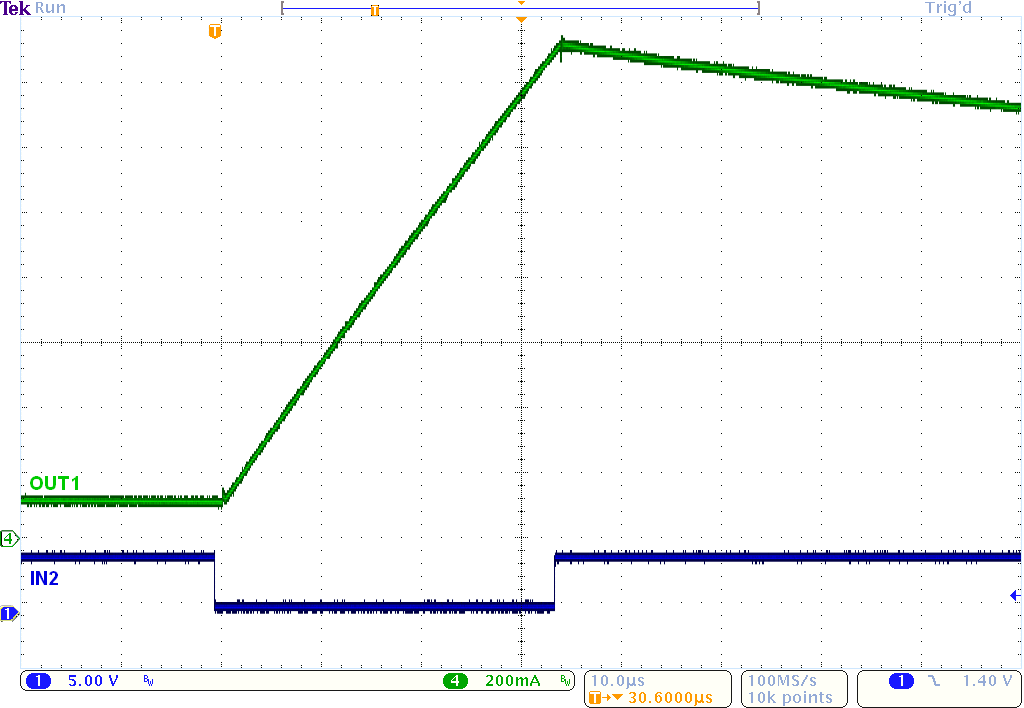
DRV8871 app_current_ramp_VM_12V_slvscy8.pngFigure 8. Current Ramp With a 2-Ω, 1 mH,
RL Load and VM = 12 V
DRV8871 app_current_ramp_VM_45V_slvscy8.pngFigure 10. Current Ramp With a 2-Ω, 1 mH,
RL Load and VM = 45 V
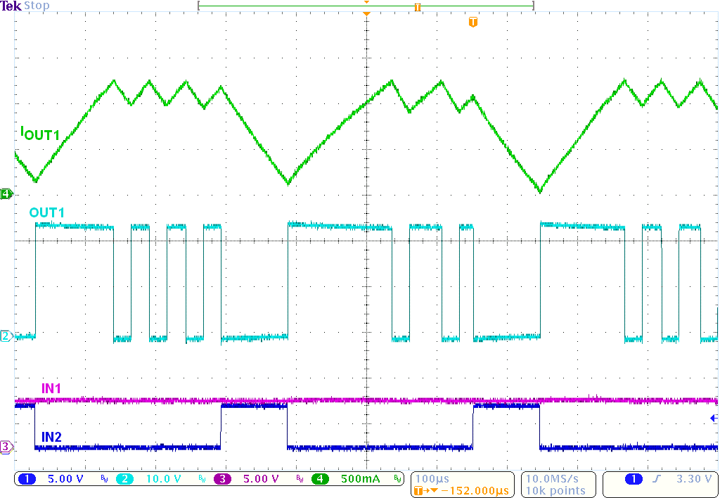
DRV8871 app_current_reg_slvscy9.pngFigure 12. Current Regulation With RILIM = 50.5 kΩ
DRV8871 app_current_ramp_VM_24V_slvscy8.pngFigure 9. Current Ramp With a 2-Ω, 1 mH,
RL Load and VM = 24 V
DRV8871 app_tPD_slvscy8.pngFigure 11. tPD
DRV8871 app_OCP_slvscy9.pngFigure 13. OCP With 45 V and the Outputs Shorted Together