SLVSCY9B August   2015  – July 2016 DRV8871

PRODUCTION DATA.  

  1. Features
  2. Applications
  3. Description
    1.     Device Images
      1.      Simplified Schematic
      2.      Peak Current Regulation
  4. Revision History
  5. Pin Configuration and Functions
    1.     Pin Functions
  6. Specifications
    1. 6.1 Absolute Maximum Ratings
    2. 6.2 ESD Ratings
    3. 6.3 Recommended Operating Conditions
    4. 6.4 Thermal Information
    5. 6.5 Electrical Characteristics
    6. 6.6 Typical Characteristics
  7. Detailed Description
    1. 7.1 Overview
    2. 7.2 Functional Block Diagram
    3. 7.3 Feature Description
      1. 7.3.1 Bridge Control
      2. 7.3.2 Sleep Mode
      3. 7.3.3 Current Regulation
      4. 7.3.4 Dead Time
      5. 7.3.5 Protection Circuits
        1. 7.3.5.1 VM Undervoltage Lockout (UVLO)
        2. 7.3.5.2 Overcurrent Protection (OCP)
        3. 7.3.5.3 Thermal Shutdown (TSD)
    4. 7.4 Device Functional Modes
      1. 7.4.1 PWM With Current Regulation
      2. 7.4.2 PWM Without Current Regulation
      3. 7.4.3 Static Inputs With Current Regulation
      4. 7.4.4 VM Control
  8. Application and Implementation
    1. 8.1 Application Information
    2. 8.2 Typical Application
      1. 8.2.1 Design Requirements
      2. 8.2.2 Detailed Design Procedure
        1. 8.2.2.1 Motor Voltage
        2. 8.2.2.2 Drive Current
      3. 8.2.3 Application Curves
  9. Power Supply Recommendations
    1. 9.1 Bulk Capacitance
  10. 10Layout
    1. 10.1 Layout Guidelines
    2. 10.2 Layout Example
    3. 10.3 Thermal Considerations
    4. 10.4 Power Dissipation
      1. 10.4.1 Heatsinking
  11. 11Device and Documentation Support
    1. 11.1 Documentation Support
      1. 11.1.1 Related Documentation
    2. 11.2 Receiving Notification of Documentation Updates
    3. 11.3 Community Resources
    4. 11.4 Trademarks
    5. 11.5 Electrostatic Discharge Caution
    6. 11.6 Glossary
  12. 12Mechanical, Packaging, and Orderable Information

Package Options

Refer to the PDF data sheet for device specific package drawings

Mechanical Data (Package|Pins)
  • DDA|8
Thermal pad, mechanical data (Package|Pins)
Orderable Information

Dead Time

When an output changes from driving high to driving low, or driving low to driving high, dead time is automatically inserted to prevent shoot-through. tDEAD is the time in the middle when the output is High-Z. If the output pin is measured during tDEAD, the voltage will depend on the direction of current. If current is leaving the pin, the voltage will be a diode drop below ground. If current is entering the pin, the voltage will be a diode drop above VM. This diode is the body diode of the high-side or low-side FET.
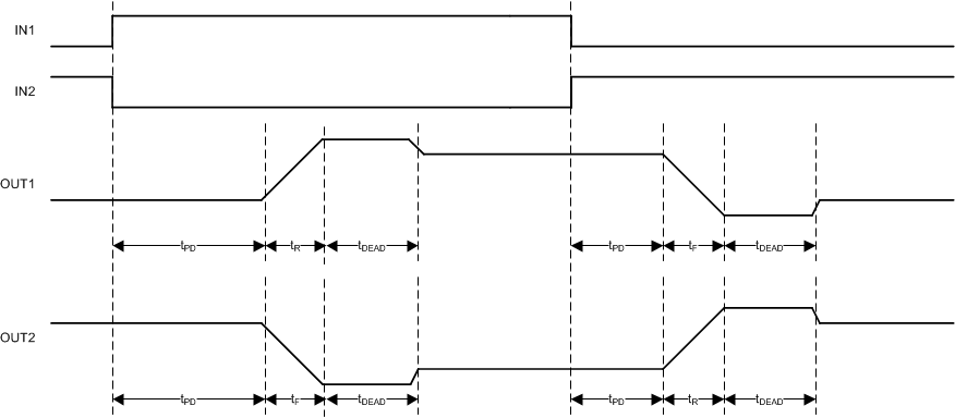
DRV8871 prop_delay_lvscy9.gifFigure 6. Propagation Delay Time