SLVSDY7B October   2017  – January 2021 DRV8873-Q1

PRODUCTION DATA  

  1. Features
  2. Applications
  3. Description
  4. Revision History
  5. Pin Configuration and Functions
    1.     Pin Functions
  6. Specifications
    1. 6.1 Absolute Maximum Ratings
    2. 6.2 ESD Ratings
    3. 6.3 Recommended Operating Conditions
    4. 6.4 Thermal Information
    5. 6.5 Electrical Characteristics
    6. 6.6 SPI Timing Requirements
    7. 6.7 Typical Characteristics
  7. Detailed Description
    1. 7.1 Overview
    2. 7.2 Functional Block Diagram
    3. 7.3 Feature Description
      1. 7.3.1 Bridge Control
        1. 7.3.1.1 Control Modes
        2. 7.3.1.2 Half-Bridge Operation
        3. 7.3.1.3 22
        4. 7.3.1.4 Internal Current Sense and Current Regulation
        5. 7.3.1.5 Slew-Rate Control
        6. 7.3.1.6 Dead Time
        7. 7.3.1.7 Propagation Delay
        8. 7.3.1.8 nFAULT Pin
        9. 7.3.1.9 nSLEEP as SDO Reference
      2. 7.3.2 Motor Driver Protection Circuits
        1. 7.3.2.1 VM Undervoltage Lockout (UVLO)
        2. 7.3.2.2 VCP Undervoltage Lockout (CPUV)
        3. 7.3.2.3 Overcurrent Protection (OCP)
          1. 7.3.2.3.1 Latched Shutdown (OCP_MODE = 00b)
          2. 7.3.2.3.2 Automatic Retry (OCP_MODE = 01b)
          3. 7.3.2.3.3 Report Only (OCP_MODE = 10b)
          4. 7.3.2.3.4 Disabled (OCP_MODE = 11b)
        4. 7.3.2.4 Open-Load Detection (OLD)
          1. 7.3.2.4.1 Open-Load Detection in Passive Mode (OLP)
          2. 7.3.2.4.2 Open-Load Detection in Active Mode (OLA)
        5. 7.3.2.5 Thermal Shutdown (TSD)
          1. 7.3.2.5.1 Latched Shutdown (TSD_MODE = 0b)
          2. 7.3.2.5.2 Automatic Recovery (TSD_MODE = 1b)
        6. 7.3.2.6 Thermal Warning (OTW)
      3. 7.3.3 Hardware Interface
        1. 7.3.3.1 MODE (Tri-Level Input)
        2. 7.3.3.2 Slew Rate
    4. 7.4 Device Functional Modes
      1. 7.4.1 Motor Driver Functional Modes
        1. 7.4.1.1 Sleep Mode (nSLEEP = 0)
        2. 7.4.1.2 Disable Mode (nSLEEP = 1, DISABLE = 1)
        3. 7.4.1.3 Operating Mode (nSLEEP = 1, DISABLE = 0)
        4. 7.4.1.4 nSLEEP Reset Pulse
    5. 7.5 Programming
      1. 7.5.1 Serial Peripheral Interface (SPI) Communication
        1. 7.5.1.1 SPI Format
        2. 7.5.1.2 SPI for a Single Slave Device
        3. 7.5.1.3 SPI for Multiple Slave Devices in Parallel Configuration
        4. 7.5.1.4 SPI for Multiple Slave Devices in Daisy Chain Configuration
    6. 7.6 Register Maps
  8. Application and Implementation
    1. 8.1 Application Information
    2. 8.2 Typical Application
      1. 8.2.1 Design Requirements
        1. 8.2.1.1 Motor Voltage
        2. 8.2.1.2 Drive Current and Power Dissipation
        3. 8.2.1.3 Sense Resistor
      2. 8.2.2 Detailed Design Procedure
        1. 8.2.2.1 Thermal Considerations
        2. 8.2.2.2 Heatsinking
      3. 8.2.3 Application Curves
  9. Power Supply Recommendations
    1. 9.1 Bulk Capacitance Sizing
  10. 10Layout
    1. 10.1 Layout Guidelines
    2. 10.2 Layout Example
  11. 11Device and Documentation Support
    1. 11.1 Documentation Support
      1. 11.1.1 Related Documentation
    2. 11.2 Receiving Notification of Documentation Updates
    3. 11.3 Support Resources
    4. 11.4 Trademarks
    5. 11.5 Electrostatic Discharge Caution
    6. 11.6 Glossary
  12. 12Mechanical, Packaging, and Orderable Information

Package Options

Mechanical Data (Package|Pins)
Thermal pad, mechanical data (Package|Pins)
Orderable Information

nSLEEP as SDO Reference

The nSLEEP pin manages the state of the device. The device goes into sleep mode with a logic-low signal, and comes out of sleep mode when the nSLEEP pin goes high. The signal level when the nSLEEP pin goes high determines the logic level on the SDO output in the SPI version of the device. A 3.3-V signal on the nSLEEP pin provides a 3.3-V output on the SDO output. A 5-V signal on the nSLEEP pin provides a 5-V output on the SDO pin. If the sleep feature is not required, the nSLEEP pin can be connected to the MCU power supply. In that case, when the MCU is powered-up, the motor driver device is also be powered-up.
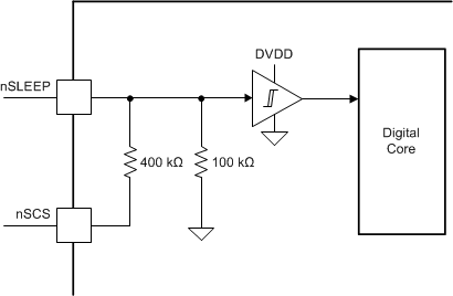
GUID-9C15325A-AAB7-4D13-9B84-3386AE1B53EE-low.gifFigure 7-11 nSCS and nSLEEP Circuit

In the SPI version of the device, if the nSLEEP reset pulse is used to clear faults, the SDO voltage reference is not available for the duration of the nSLEEP reset pulse. No data can be transmitted on the SDO line for the duration when the nSLEEP pin is held low. Therefore, TI recommends using the CLR_FLT bit in the IC3 control register to clear the faults.