SLVSDS6B August   2019  – January 2021 DRV8876-Q1

PRODUCTION DATA  

  1. Features
  2. Applications
  3. Description
  4. Revision History
  5. Pin Configuration and Functions
    1.     Pin Functions
  6. Specifications
    1. 6.1 Absolute Maximum Ratings
    2. 6.2 ESD Ratings
    3. 6.3 Recommended Operating Conditions
    4. 6.4 Thermal Information
    5. 6.5 Electrical Characteristics
    6. 6.6 Typical Characteristics
  7. Detailed Description
    1. 7.1 Overview
    2. 7.2 Functional Block Diagram
    3. 7.3 Feature Description
      1. 7.3.1 External Components
      2. 7.3.2 Control Modes
        1. 7.3.2.1 PH/EN Control Mode (PMODE = Logic Low)
        2. 7.3.2.2 PWM Control Mode (PMODE = Logic High)
        3. 7.3.2.3 Independent Half-Bridge Control Mode (PMODE = Hi-Z)
      3. 7.3.3 Current Sense and Regulation
        1. 7.3.3.1 Current Sensing
        2. 7.3.3.2 Current Regulation
          1. 7.3.3.2.1 Fixed Off-Time Current Chopping
          2. 7.3.3.2.2 Cycle-By-Cycle Current Chopping
      4. 7.3.4 Protection Circuits
        1. 7.3.4.1 VM Supply Undervoltage Lockout (UVLO)
        2. 7.3.4.2 VCP Charge Pump Undervoltage Lockout (CPUV)
        3. 7.3.4.3 OUTx Overcurrent Protection (OCP)
        4. 7.3.4.4 Thermal Shutdown (TSD)
        5. 7.3.4.5 Fault Condition Summary
      5. 7.3.5 Pin Diagrams
        1. 7.3.5.1 Logic-Level Inputs
        2. 7.3.5.2 Tri-Level Inputs
        3. 7.3.5.3 Quad-Level Inputs
    4. 7.4 Device Functional Modes
      1. 7.4.1 Active Mode
      2. 7.4.2 Low-Power Sleep Mode
      3. 7.4.3 Fault Mode
  8. Application and Implementation
    1. 8.1 Application Information
    2. 8.2 Typical Application
      1. 8.2.1 Primary Application
        1. 8.2.1.1 Design Requirements
        2. 8.2.1.2 Detailed Design Procedure
          1. 8.2.1.2.1 Current Sense and Regulation
          2. 8.2.1.2.2 Power Dissipation and Output Current Capability
          3. 8.2.1.2.3 Thermal Performance
            1. 8.2.1.2.3.1 Steady-State Thermal Performance
            2. 8.2.1.2.3.2 Transient Thermal Performance
        3. 8.2.1.3 Application Curves
      2. 8.2.2 Alternative Application
        1. 8.2.2.1 Design Requirements
        2. 8.2.2.2 Detailed Design Procedure
          1. 8.2.2.2.1 Current Sense and Regulation
        3. 8.2.2.3 Application Curves
  9. Power Supply Recommendations
    1. 9.1 Bulk Capacitance
  10. 10Layout
    1. 10.1 Layout Guidelines
    2. 10.2 Layout Example
      1. 10.2.1 HTSSOP Layout Example
  11. 11Device and Documentation Support
    1. 11.1 Documentation Support
      1. 11.1.1 Related Documentation
    2. 11.2 Receiving Notification of Documentation Updates
    3. 11.3 Community Resources
    4. 11.4 Trademarks
  12. 12Mechanical, Packaging, and Orderable Information

Package Options

Refer to the PDF data sheet for device specific package drawings

Mechanical Data (Package|Pins)
  • PWP|16
Thermal pad, mechanical data (Package|Pins)
Orderable Information
Transient Thermal Performance

The motor driver may experience different transient driving conditions that cause large currents to flow for a short duration of time. These may include

  • Motor start-up when the rotor is not yet spinning at full speed.
  • Fault conditions when there is a supply or ground short to one of the motor outputs, and the device goes into and out of overcurrent protection.
  • Briefly energizing a motor or solenoid for a limited time, then de-energizing.

For these transient cases, the duration of drive time is another factor that impacts thermal performance. In transient cases, the thermal impedance parameter ZθJA denotes the junction-to-ambient thermal performance. Figure 8-7 and Figure 8-8 show the simulated thermal impedances for 1-oz and 2-oz copper layouts for the HTSSOP package. These graphs indicate better thermal performance with short current pulses. For short periods of drive time, the device die size and package dominates the thermal performance. For longer drive pulses, board layout has a more significant impact on thermal performance. Both graphs show the curves for thermal impedance split due to number of layers and copper area as the duration of the drive pulse duration increases. Long pulses can be considered steady-state performance.
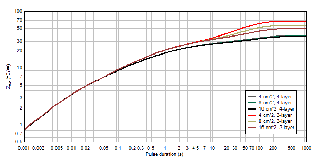
GUID-28E8B2A4-5FD3-4F81-B72A-7E03005F78FC-low.gifFigure 8-7 HTSSOP package junction-to-ambient thermal impedance for 1-oz copper layouts
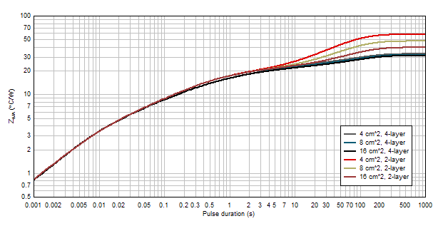
GUID-94EC55E8-822D-4966-BFC8-BAB27F7420DF-low.gifFigure 8-8 HTSSOP package Junction-to-ambient thermal impedance for 2-oz copper layouts