SLVSFE6A August   2019  – April 2021 DRV8876N

PRODUCTION DATA  

  1. Features
  2. Applications
  3. Description
  4. Revision History
  5. Pin Configuration and Functions
    1.     Pin Functions
  6. Specifications
    1. 6.1 Absolute Maximum Ratings
    2. 6.2 ESD Ratings
    3. 6.3 Recommended Operating Conditions
    4. 6.4 Thermal Information
    5. 6.5 Electrical Characteristics
    6. 6.6 Typical Characteristics
  7. Detailed Description
    1. 7.1 Overview
    2. 7.2 Functional Block Diagram
    3. 7.3 Feature Description
      1. 7.3.1 External Components
      2. 7.3.2 Control Modes
        1. 7.3.2.1 PH/EN Control Mode (PMODE = Logic Low)
        2. 7.3.2.2 PWM Control Mode (PMODE = Logic High)
        3. 7.3.2.3 Independent Half-Bridge Control Mode (PMODE = Hi-Z)
      3. 7.3.3 Protection Circuits
        1. 7.3.3.1 VM Supply Undervoltage Lockout (UVLO)
        2. 7.3.3.2 VCP Charge Pump Undervoltage Lockout (CPUV)
        3. 7.3.3.3 OUTx Overcurrent Protection (OCP)
        4. 7.3.3.4 Thermal Shutdown (TSD)
        5. 7.3.3.5 Fault Condition Summary
      4. 7.3.4 Pin Diagrams
        1. 7.3.4.1 Logic-Level Inputs
        2. 7.3.4.2 Tri-Level Inputs
        3. 7.3.4.3 Quad-Level Inputs
    4. 7.4 Device Functional Modes
      1. 7.4.1 Active Mode
      2. 7.4.2 Low-Power Sleep Mode
      3. 7.4.3 Fault Mode
  8. Application and Implementation
    1. 8.1 Application Information
    2. 8.2 Typical Application
      1. 8.2.1 Primary Application
        1. 8.2.1.1 Design Requirements
        2. 8.2.1.2 Detailed Design Procedure
          1. 8.2.1.2.1 Power Dissipation and Output Current Capability
          2. 8.2.1.2.2 Thermal Performance
            1. 8.2.1.2.2.1 Steady-State Thermal Performance
            2. 8.2.1.2.2.2 Transient Thermal Performance
        3. 8.2.1.3 Application Curves
      2. 8.2.2 Alternative Application
        1. 8.2.2.1 Design Requirements
        2. 8.2.2.2 Detailed Design Procedure
        3. 8.2.2.3 Application Curves
  9. Power Supply Recommendations
    1. 9.1 Bulk Capacitance
  10. 10Layout
    1. 10.1 Layout Guidelines
    2. 10.2 Layout Example
      1. 10.2.1 HTSSOP Layout Example
  11. 11Device and Documentation Support
    1. 11.1 Documentation Support
      1. 11.1.1 Related Documentation
    2. 11.2 Receiving Notification of Documentation Updates
    3. 11.3 Community Resources
    4. 11.4 Trademarks
  12. 12Mechanical, Packaging, and Orderable Information

Package Options

Mechanical Data (Package|Pins)
Thermal pad, mechanical data (Package|Pins)
Orderable Information

Description

The DRV8876N is an integrated motor driver with N-channel H-bridge, charge pump, and protection circuitry. The charge pump improves efficiency by supporting N-channel MOSFET half bridges and 100% duty cycle driving. The family of devices come in pin-to-pin RDS(on) variants to support different loads with minimal design changes.

A low-power sleep mode achieves ultra-low quiescent current draw by shutting down most of the internal circuitry. Internal protection features include supply undervoltage lockout, charge pump undervoltage, output overcurrent, and device overtemperature. Fault conditions are indicated on nFAULT.

View our full portfolio of brushed motor drivers on ti.com.

Device Information (1)
PART NUMBER PACKAGE BODY SIZE (NOM)
DRV8876N HTSSOP (16) 5.00 mm × 4.40 mm
For all available packages, see the orderable addendum at the end of the data sheet.
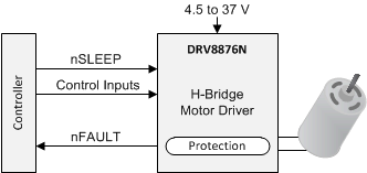
GUID-11C9B0FF-A9C3-4A9D-AFB5-8B8D1DC909FA-low.gif Simplified Schematic