SLVSD18C June 2015 – August 2017 DRV8880
PRODUCTION DATA.
- 1 Features
- 2 Applications
- 3 Description
- 4 Revision History
- 5 Pin Configuration and Functions
- 6 Specifications
-
7 Detailed Description
- 7.1 Overview
- 7.2 Functional Block Diagram
- 7.3
Feature Description
- 7.3.1 Stepper Motor Driver Current Ratings
- 7.3.2 PWM Motor Drivers
- 7.3.3 Microstepping Indexer
- 7.3.4 Current Regulation
- 7.3.5
Decay Modes
- 7.3.5.1 Mode 1: Slow Decay for Increasing and Decreasing Current
- 7.3.5.2 Mode 2: Slow Decay for Increasing Current, Mixed Decay for Decreasing current
- 7.3.5.3 Mode 3: Mixed Decay for Increasing and Decreasing Current
- 7.3.5.4 Mode 4: Slow Decay for Increasing Current, Fast Decay for Decreasing current
- 7.3.5.5 Mode 5: Fast Decay for Increasing and Decreasing Current
- 7.3.6 Smart Tune
- 7.3.7 Adaptive Blanking Time
- 7.3.8 Charge Pump
- 7.3.9 LDO Voltage Regulator
- 7.3.10 Logic and Tri-Level Pin Diagrams
- 7.3.11 Power Supplies and Input Pins
- 7.3.12 Protection Circuits
- 7.3.13 VM UVLO (UVLO2)
- 7.3.14 Logic Undervoltage (UVLO1)
- 7.3.15 VCP Undervoltage Lockout (CPUV)
- 7.3.16 Thermal Shutdown (TSD)
- 7.3.17 Overcurrent Protection (OCP)
- 7.4 Device Functional Modes
- 8 Application and Implementation
- 9 Power Supply Recommendations
- 10Layout
- 11Device and Documentation Support
- 12Mechanical, Packaging, and Orderable Information
Package Options
Refer to the PDF data sheet for device specific package drawings
Mechanical Data (Package|Pins)
- RHR|28
- PWP|28
Thermal pad, mechanical data (Package|Pins)
Orderable Information
7.3.10 Logic and Tri-Level Pin Diagrams
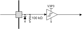
The diagram below gives the input structure for logic-level pins STEP, DIR, ENABLE, nSLEEP, TRQ0, TRQ1, and ATE:
 Figure 23. Logic-level Input Pin Diagram
 Tri-level logic pins TOFF, M0, M1, DECAY0, and DECAY1 have the following structure:
 Figure 24. Tri-level Input Pin Diagram