SLVSDO1C January 2017 – March 2020 DRV8886AT
PRODUCTION DATA.
- 1 Features
- 2 Applications
- 3 Description
- 4 Revision History
- 5 Pin Configuration and Functions
- 6 Specifications
-
7 Detailed Description
- 7.1 Overview
- 7.2 Functional Block Diagram
- 7.3
Feature Description
- 7.3.1 Stepper Motor Driver Current Ratings
- 7.3.2 PWM Motor Drivers
- 7.3.3 Microstepping Indexer
- 7.3.4 Current Regulation
- 7.3.5 Controlling RREF With an MCU DAC
- 7.3.6 Decay Modes
- 7.3.7 Blanking Time
- 7.3.8 Charge Pump
- 7.3.9 Linear Voltage Regulators
- 7.3.10 Logic and Multi-Level Pin Diagrams
- 7.3.11 Protection Circuits
- 7.4 Device Functional Modes
- 8 Application and Implementation
- 9 Power Supply Recommendations
- 10Layout
- 11Device and Documentation Support
- 12Mechanical, Packaging, and Orderable Information
Package Options
Mechanical Data (Package|Pins)
Thermal pad, mechanical data (Package|Pins)
Orderable Information
3 Description
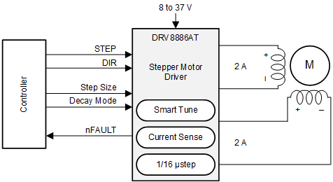
The DRV8886AT is a stepper motor driver for industrial and consumer end equipment applications. The device is fully integrated with two N-channel power MOSFET H-bridge drivers, a microstepping indexer, and integrated current sensing. The DRV8886AT is capable of driving up to 2-A full scale or 1.4-A rms output current (24-V and TA = 25°C, dependent on PCB design).
The DRV8886AT uses an internal current sense architecture to eliminate the need for two external power sense resistors saving PCB area and system cost. The DRV8886AT uses an internal PWM current regulation scheme adjustable between smart tune adaptive decay technology, slow, and mixed decay options. Smart tune adaptive decay technology automatically adjusts for optimal current regulation performance and compensates for motor variation and aging effects.
A simple STEP/DIR interface allows an external controller to manage the direction and step rate of the stepper motor. The device can be configured in different step modes ranging from full-step to 1/16 microstepping. A low-power sleep mode is provided for very low standby quiescent standby current using a dedicated nSLEEP pin.
Device protection features are provided for supply undervoltage, charge pump faults, overcurrent, short circuits, and overtemperature. Fault conditions are indicated by the nFAULT pin.
Device Information(1)
| PART NUMBER | PACKAGE | BODY SIZE (NOM) |
|---|---|---|
| DRV8886AT | HTSSOP (24) | 7.80 mm × 4.40 mm |
| WQFN (28) | 5.50 mm × 3.5 mm |
- For all available packages, see the orderable addendum at the end of the data sheet.
Simplified Schematic
