DS125BR401A Low-Power 12 Gbps 4-Lane Linear Repeater With Equalization
1 Features
- Low 65-mW/Channel (Typ) Power Consumption, With Option to Power Down Unused Channels
- Linear Equalization allows for Link Training in PCIe and SAS
- Supports Out-of-Band (OOB) Signaling
- Advanced Signal Conditioning B-Side I/O
- Receive CTLE up to 24 dB at 6 GHz
- Transmit (Tx) DE > 10 dB
- Tx Output Voltage: 700 mV to 1400 mV
- Advanced Signal Conditioning A-Side I/O
- Receive CTLE up to 10 dB at 6 GHz
- Linear output drive
- Output voltage range over 1200mV Programmable via Terminal Selection, EEPROM, or SMBus Interface
- Single Supply Voltage: 2.5 V or 3.3 V
- −40°C to 85°C Operating Temperature Range
- 4 kV HBM ESD Rating
- Flow-Thru Layout in 10mmx5.5mm 54-Terminal Leadless WQFN Package
2 Applications
- SAS/SATA
- PCI Express
- Other Proprietary Interfaces up to 12 Gbps
3 Description
The DS125BR401A is an extremely low-power high-performance repeater/redriver designed to support four lanes carrying high speed interface up to 12 Gbps. The B-Side receiver's continuous time linear equalizers (CTLE) provide high frequency boost of up to +24 dB at 6 GHz (12 Gbps) and are capable of opening an input eye that is completely closed due to inter symbol interference (ISI) induced by interconnect medium such as backplane traces or twinaxial copper cables. The programmable equalization allows maximum flexibility in the physical placement within the interconnect channel. The A-Side channel has a 10 dB linear equalizer and linear output driver.
The A-Side channel has a settable 3-10 dB linear equalizer coupled to a linear output driver. When operating in SAS-3 and PCIe Gen-3 applications the DS125BR401A preserves transmit signal characteristics allowing the host controller and the end point to negotiate transmit equalizer coefficients. This transparency to the link training protocol aides system level interoperability and minimum latency.
The programmable settings can be applied easily via Terminals, software (SMBus or I2C), or loaded via an external EEPROM. In EEPROM mode, the configuration information is automatically loaded on power up, which eliminates the need for an external microprocessor or software driver.
Device Information
| ORDER NUMBER | PACKAGE | BODY SIZE |
|---|---|---|
| DS125BR401ANJY | WQFN (48) | 10 mm x 5,5 mm |
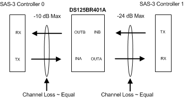
SAS-3 Application
5 Terminal Configuration and Functions
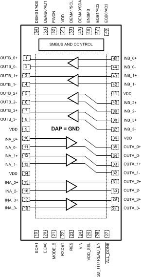
Terminal Functions(1)
| TERMINAL NAME | TERMINAL NUMBER | I/O, TYPE | TERMINAL DESCRIPTION |
|---|---|---|---|
| DIFFERENTIAL HIGH SPEED I/O | |||
| INB_0+, INB_0- , INB_1+, INB_1-, INB_2+, INB_2-, INB_3+, INB_3- |
45, 44, 43, 42 40, 39, 38, 37 |
I | Inverting and non-inverting CML differential inputs to the equalizer. On-chip 50Ω termination resistor connects INB_n+ to VDD and INB_n- to VDD when enabled. AC coupling required on high-speed I/O |
| OUTB_0+, OUTB_0-, OUTB_1+, OUTB_1-, OUTB_2+, OUTB_2-, OUTB_3+, OUTB_3- |
1, 2, 3, 4 5, 6, 7, 8 |
O | Inverting and non-inverting 50Ω driver outputs with de-emphasis. Compatible with AC coupled CML inputs. AC coupling required on high-speed I/O |
| INA_0+, INA_0- , INA_1+, INA_1-, INA_2+, INA_2-, INA_3+, INA_3- |
10, 11, 12, 13 15, 16, 17, 18 |
I | Inverting and non-inverting CML differential inputs to the equalizer. On-chip 50Ω termination resistor connects INA_n+ to VDD and INA_n- to VDD when enabled. AC coupling required on high-speed I/O |
| OUTA_0+, OUTA_0-, OUTA_1+, OUTA_1-, OUTA_2+, OUTA_2-, OUTA_3+, OUTA_3- |
35, 34, 33, 32 31, 30, 29, 28 |
O | Inverting and non-inverting 50Ω driver outputs. Compatible with AC coupled CML inputs. AC coupling required on high-speed I/O |
| CONTROL TERMINALS — SHARED (LVCMOS) | |||
| ENSMB | 48 | I, LVCMOS | System Management Bus (SMBus) enable Terminal Tie 1kΩ to VDD = Register Access SMBus Slave mode FLOAT = Read External EEPROM (Master SMBUS Mode) Tie 1kΩ to GND = Terminal Mode |
| ENSMB = 1 (SMBus MODE) | |||
| SCL | 50 | I, LVCMOS, O, OPEN Drain |
ENSMB Master or Slave mode SMBus clock input Terminal is enabled (slave mode). Clock output when loading EEPROM configuration (master mode). |
| SDA | 49 | I, LVCMOS, O, OPEN Drain |
ENSMB Master or Slave mode The SMBus bidirectional SDA Terminal is enabled. Data input or open drain (pull-down only) output. |
| AD0-AD3 | 54, 53, 47, 46 | I, LVCMOS | ENSMB Master or Slave mode SMBus Slave Address Inputs. In SMBus mode, these Terminals are the user set SMBus slave address inputs. |
| READ_EN | 26 | I, LVCMOS | When using an External EEPROM, a logic low on this terminal starts the load from the external EEPROM |
| ENSMB = 0 (TERMINAL MODE) | |||
| EQA0, EQA1 EQB0, EQB1 |
20, 19 46, 47 |
I, 4-LEVEL, LVCMOS |
EQA[1:0] and EQB[1:0] control the level of equalization of the A/B directions. The Terminals are defined as EQx[1:0] only when ENSMB is de-asserted (low). Each of the 4 A/B channels have the same level unless controlled by the SMBus control registers. When ENSMB goes high the SMBus registers provide independent control of each lane. The EQB[1:0] Terminals are converted to SMBus AD2, AD3 inputs. See Table 5. |
| DEMB0, DEMB1 | 53, 54 | I, 4-LEVEL, LVCMOS |
DEMB[1:0] controls the level of de-emphasis of CHB outputs. The Terminals are defined as DEMB[1:0] only when ENSMB is de-asserted (low). Each of the 4 B channels have the same level unless controlled by the SMBus control registers. When ENSMB goes high the SMBus registers provide independent control of each lane. The DEMB[1:0] Terminals are converted to AD0, AD1 inputs. See Table 7. |
| MODE_B | 21 | I, 4-LEVEL, LVCMOS |
MODE_B control Terminal selects operating modes for the INB-OUTB Channels. Tie 1kΩ to GND = GEN 1,2 and SAS 1,2 Float = Auto Mode Select (for PCIe) Tie 20kΩ to GND = SAS-3 and GEN-3 without De-emphasis Tie 1kΩ to VDD = SAS-3 and GEN-3 with De-emphasis See Table 4. |
| DEMA0, DEMA1 | 49, 50 | I, 4-LEVEL, LVCMOS |
DEMA[1:0] controls the CHA output amplitude. The Terminals are defined as DEMA[1:0] only when ENSMB is de-asserted (low). Each of the 4 A channels have the same level unless controlled by the SMBus control registers. When ENSMB goes high the SMBus registers provide independent control of each lane and the DEMA[1:0] Terminals are converted to SCL and SDA. See Table 7. |
| SD_TH | 26 | I, 4-LEVEL, LVCMOS |
Controls the internal Signal Detect Threshold on the INB-OUTB Channels. For CHB, the signal detect is used to bring the output into and out of IDLE. This allows the OOB signaling to pass with minimal distortion. See Table 3. |
| CONTROL TERMINALS — BOTH TERMINAL AND SMBus MODES (LVCMOS) | |||
| RXDET | 22 | I, 4-LEVEL, LVCMOS |
The RXDET Terminal controls the receiver detect function. Depending on the input level, a 50Ω or >50KΩ termination to the power rail is enabled. In SAS/SATA system RXDET should be set to a Logic "1" state to keep the termination always enabled. See Table 2. |
| RES | 23 | I, 4-LEVEL, LVCMOS |
Reserved: This input must be left Floating. |
| VDD_SEL | 25 | I, FLOAT | Controls the internal regulator Float = 2.5V mode Tie GND = 3.3V mode |
| PWDN | 52 | I, LVCMOS | Tie High = Low power - power down Tie GND = Normal Operation See Table 2. |
| ALL_DONE | 27 | O, LVCMOS | Valid Register Load Status Output HIGH = External EEPROM load failed or incomplete LOW = External EEPROM load passed |
| POWER | |||
| VIN | 24 | Power | In 3.3V mode, feed 3.3V to VIN In 2.5V mode, leave floating. |
| VDD | 9, 14,36, 41, 51 | Power | Power supply Terminals CML/analog 2.5V mode, connect to 2.5V 3.3V mode, connect 0.1 µF cap to each VDD Terminal and GND |
| GND | DAP | Power | Ground pad (DAP - die attach pad). |
Input edge rate for LVCMOS/FLOAT inputs must be faster than 50 ns from 10–90%.
For 3.3V mode operation, VIN Terminal input = 3.3V and the logic "1" reference for the 4-level input is 3.3V.
For 2.5V mode operation, VDD Terminal output= 2.5V and the logic "1" reference for the 4-level input is 2.5V.
6 Specifications
6.1 Absolute Maximum Ratings(1)
| MIN | MAX | UNIT | ||
|---|---|---|---|---|
| Supply Voltage (VDD - 2.5V) | -0.5 | +2.75 | V | |
| Supply Voltage (VIN - 3.3V) | -0.5 | +4.0 | V | |
| LVCMOS Input/Output Voltage | -0.5 | +4.0 | V | |
| CML Input Voltage | -0.5V to (VDD+0.5) | |||
| CML Input Current | -30 | +30 | mA | |
6.2 Handling Ratings
| MIN | MAX | UNIT | ||
|---|---|---|---|---|
| ESDHBM | HBM, STD - JESD22-A114F | 4 | kV | |
| ESDCDM | CDM, STD - JESD22-C101-D | 1 | kV | |
| Tstg | Storage Temperature Range | -40 | 125 | °C |
| Tsolder | Lead Temperature Range Soldering (4 sec.) (1) | 260 | °C |
6.3 Recommended Operating Conditions
| MIN | TYP | MAX | UNIT | |
|---|---|---|---|---|
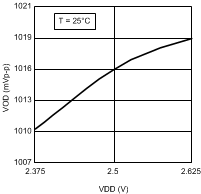
| Supply Voltage (2.5V mode) | 2.375 | 2.5 | 2.625 | V |
| Supply Voltage (3.3V mode) | 3.0 | 3.3 | 3.6 | V |
| Ambient Temperature | -40 | 25 | +85 | °C |
| SMBus (SDA, SCL) | 3.6 | V | ||
| Supply Noise up to 50 MHz(1) | 100 | mVp-p |
6.4 Thermal Information
| THERMAL METRIC(1) | DS125BR401A | UNIT | |
|---|---|---|---|
| WQFN | |||
| 54 TERMINALS | |||
| RθJA | Junction-to-ambient thermal resistance | 26.6 | °C/W |
| RθJCtop | Junction-to-case (top) thermal resistance | 10.8 | |
| RθJB | Junction-to-board thermal resistance | 4.4 | |
| ψJT | Junction-to-top characterization parameter | 0.2 | |
| ψJB | Junction-to-board characterization parameter | 4.3 | |
| RθJCbot | Junction-to-case (bottom) thermal resistance | 1.5 | |
6.5 Electrical Characteristics
| PARAMETER | TEST CONDITIONS | MIN | TYP | MAX | UNIT | |
|---|---|---|---|---|---|---|
| POWER | ||||||
| IDD | Current Consumption | DEM0 = Float, ,DEM1 = Float EQ = 0, VOD = 0.8VP-P, RXDET = 1, PWDN = 0 |
200 | 280 | mA | |
| Power Down Current Consumption | PWDN = 1 | 14 | 27 | mA | ||
| VDD | Integrated LDO Regulator | VIN = 3.0 - 3.6 V | 2.375 | 2.5 | 2.625 | V |
| LVCMOS / LVTTL DC SPECIFICATIONS | ||||||
| Vih25 | High Level Input Voltage | 2.5 V Supply Mode | 1.7 | VDD | V | |
| Vih33 | High Level Input Voltage | 3.3 V Supply Mode | 1.7 | VIN | V | |
| Vil | Low Level Input Voltage | 0 | 0.7 | V | ||
| Voh | High Level Output Voltage (ALL_DONE Terminal) |
Ioh = −4mA | 2.0 | V | ||
| Vol | Low Level Output Voltage (ALL_DONE Terminal) |
Iol = 4mA | 0.4 | V | ||
| Iih | Input High Current (PWDN Terminal) | VIN = 3.6 V, LVCMOS = 3.6 V |
-15 | +15 | uA | |
| Iil | Input Low Current (PWDN Terminal) | VIN = 3.6 V, LVCMOS = 0 V |
-15 | +15 | uA | |
| 4-LEVEL INPUT DC SPECIFICATIONS | ||||||
| Iih | Input High Current with internal resistors (4–level input Terminal) |
VIN = 3.6 V, LVCMOS = 3.6 V |
+20 | +150 | uA | |
| Iil | Input Low Current with internal resistors (4–level input Terminal) |
VIN = 3.6 V, LVCMOS = 0 V |
-160 | -40 | uA | |
| Vth | Threshold 0 / R | VDD = 2.5V (2.5V supply mode) Internal LDO Disabled See Table 1 for details |
0.45 | V | ||
| Threshold R / Float | 1.2 | |||||
| Threshold Float / 1 | 2 | |||||
| Threshold 0 / R | VIN = 3.3V (3.3V supply mode) Internal LDO Enabled See Table 1 for details. |
0.6 | V | |||
| Threshold R / Float | 1.6 | |||||
| Threshold Float / 1 | 2.6 | |||||
| CML RECEIVER INPUTS (IN_n+, IN_n-) | ||||||
| RLRX-diff | RX Differential return loss | SDD11 10 MHz | -19 | dB | ||
| SDD11 2 GHz | -14 | |||||
| SDD11 6-11.1 GHz | -8 | |||||
| RLRX-cm | RX Common mode return loss | 0.05 - 5 GHz | -10 | dB | ||
| ZRX-dc | RX DC common mode impedance | Tested at VDD = 2.5 V | 40 | 50 | 60 | Ω |
| ZRX-diff-dc | RX DC differential mode impedance | Tested at VDD = 2.5 V | 80 | 100 | 120 | Ω |
| VRX-signal-det-diff-pp | Signal detect assert level for active data signal | SD_TH = F (float), 0101 pattern at 12 Gbps |
50 | mVp-p | ||
| VRX-idle-det-diff-pp | Signal detect de-assert level for electrical idle | SD_TH = F (float), 0101 pattern at 12 Gbps |
37 | mVp-p | ||
| HIGH SPEED OUTPUTS | ||||||
| TTX-RISE-FALL | Transmitter rise/fall time (3) | 20% to 80% of differential output voltage | 40 | ps | ||
| TRF-MISMATCH | Transmitter rise/fall mismatch | 20% to 80% of differential output voltage | 0.01 | UI | ||
| RLTX-DIFF | TX Differential return loss | SDD22 10 MHz - 2 GHz | -15 | dB | ||
| SDD22 5.5 GHz | -12 | |||||
| SDD22 11.1 GHz | -10 | dB | ||||
| RLTX-CM | TX Common mode return loss | 0.05 - 5 GHz | -10 | dB | ||
| ZTX-DIFF-DC | DC differential TX impedance | 100 | Ω | |||
| ITX-SHORT | Transmitter short circuit current limit | Total current, output shorted to VDD or GND | 20 | mA | ||
| VTX-CM-DC-ACTIVE-IDLE-DELTA | Absolute delta of DC common mode voltage during L0 and electrical idle | 100 | mV | |||
| VTX-CM-DC-LINE-DELTA | Absolute delta of DC common mode voltage between TX+ and TX- | 25 | mV | |||
| HIGH SPEED OUTPUTS (A-CHANNELS) | ||||||
| VTXA-diff1-pp | Output Voltage Differential Swing | Differential measurement with OUTA_n+ and OUTA_n-, AC-Coupled and terminated by 50Ω to GND, Inputs AC-Coupled, VID = 600 mVp-p VOD = 001'b (800mV) |
375 | 465 | 600 | mVp-p |
| VTXA-diff2-pp | Output Voltage Differential Swing | Differential measurement with OUTA_n+ and OUTA_n-, AC-Coupled and terminated by 50Ω to GND, Inputs AC-Coupled, VID = 1000 mVp-p VOD = 001'b (800mV) |
550 | 675 | 825 | mVp-p |
| VTXA-diff3-pp | Output Voltage Differential Swing | Differential measurement with OUTA_n+ and OUTA_n-, AC-Coupled and terminated by 50Ω to GND, Inputs AC-Coupled, VID = 600 mVp-p DEMA[1:0] = 10, VOD = 1300mV |
475 | 600 | 750 | Vp-p |
| VTXA-diff4-pp | Output Voltage Differential Swing | Differential measurement with OUTA_n+ and OUTA_n-, AC-Coupled and terminated by 50Ω to GND, Inputs AC-Coupled, VID = 1000 mVp-p VOD = 110'b (1300mV) |
775 | 915 | 1125 | Vp-p |
| TTXA-IDLE-DATA | Time to transition to valid differential signal after idle | VID = 1.0 Vp-p, 3 Gbps | 0.04 | ns | ||
| TTXA-DATA-IDLE | Time to transition to idle after differential signal | VID = 1.0 Vp-p, 3 Gbps | 0.70 | ns | ||
| TPDEQA | Differential propagation delay - Channel A | EQ = Level 1 to Level 4 | 80 | ps | ||
| HIGH SPEED OUTPUTS (B-CHANNELS) | ||||||
| VTXB-diff1-pp | Output Voltage Differential Swing | Differential measurement with OUTB_n+ and OUTB_n-, AC-Coupled and terminated by 50Ω to GND, Inputs AC-Coupled, VID = 1.0 Vp-p, MODE_B = 1 DEMB1 = 0, DEMB0 = 1(4) |
0.8 | 1.0 | 1.2 | Vp-p |
| VTXB-diff2-pp | Output Voltage Differential Swing | Differential measurement with OUTB_n+ and OUTB_n-, AC-Coupled and terminated by 50Ω to GND, Inputs AC-Coupled, VID = 1.0 Vp-p, MODE_B = 0 DEMB1 = 0, DEMB0 = R |
670 | 820 | 930 | mVp-p |
| VTXB-diff3-pp | Output Voltage Differential Swing | Differential measurement with OUTB_n+ and OUTB_n-, AC-Coupled and terminated by 50Ω to GND, Inputs AC-Coupled, VID = 1.0 Vp-p, MODE_B = 0 DEMB1 = R, DEMB0 = FLOAT |
950 | 1140 | 1250 | mVp-p |
| VTXB-de-ratio_3.5 | TX de-emphasis ratio | VOD = 1.0 Vp-p, DEM0 = 0, DEM1 = R, MODE_B = 0 OUTB_n only Gen 1 & 2 mode |
−3.5 | dB | ||
| VTXB-de-ratio_6 | TX de-emphasis ratio | VOD = 1.0 Vp-p, DEM0 = R, DEM1 = R, MODE_B = 0 OUTB_n only in Gen 1 & 2 mode |
−6 | dB | ||
| TTXB-IDLE-DATA | Time to transition to valid differential signal after idle | VID = 1.0 Vp-p, 3 Gbps | 3.5 | ns | ||
| TTXB-DATA-IDLE | Time to transition to idle after differential signal | VID = 1.0 Vp-p, 3 Gbps | 5.0 | ns | ||
| TPDEQB | Differential propagation delay - Channel B | EQ = 00(2) | 135 | ps | ||
| EQUALIZATION (A-CHANNELS) | ||||||
| DJE1A | Residual deterministic jitter at 6 Gbps | 5” Differential Stripline, 5mil trace width, FR4, VID = 0.8 Vp-p, PRBS15, EQ = 01'h, VOD = 1.3V, DEM = 0 dB |
0.06 | UI | ||
| DJE3A | Residual deterministic jitter at 12 Gbps | 5” Differential Stripline, 5mil trace width, FR4, VID = 0.8 Vp-p, PRBS15, EQ = 01'h, VOD = 1.3V, DEM = 0 dB |
0.12 | UI | ||
| EQUALIZATION (B-CHANNELS) | ||||||
| DJE1B | Residual deterministic jitter at 12 Gbps | 30” Differential Stripline, 5mil trace width, FR4, VID = 0.6 Vp-p, PRBS15, EQ = 07'h, DEM = 0 dB |
0.18 | UI | ||
| DJE2B | Residual deterministic jitter at 12 Gbps | 5 meters 30 awg cable, VID = 0.6 Vp-p, PRBS15, EQ = 07'h, DEM = 0 dB |
0.25 | UI | ||
| DE-EMPHASIS (B-CHANNELS, GEN 1&2 MODE ONLY) | ||||||
| DJD1 | Residual deterministic jitter at 12 Gbps | Input Channel: 20" Differential Stripline, 5mil trace width, FR4, Output Channel: 10” Differential Stripline, 5mil trace width, FR4, VID = 0.6 Vp-p, PRBS15, EQ = 03'h, VOD = 1.0 Vp-p, DEMB = −3.5 dB |
0.1 | UI | ||
6.6 Electrical Characteristics — Serial Management Bus Interface
Over recommended operating supply and temperature ranges unless other specified.| PARAMETER | TEST CONDITIONS | MIN | TYP | MAX | UNIT | |
|---|---|---|---|---|---|---|
| SERIAL BUS INTERFACE DC SPECIFICATIONS | ||||||
| VIL | Data, Clock Input Low Voltage | 0.8 | V | |||
| VIH | Data, Clock Input High Voltage | 2.1 | 3.6 | V | ||
| VOL | Output Low Voltage | SDA or SCL, IOL = 1.25 mA | 0 | 0.36 | V | |
| VDD | Nominal Bus Voltage | 2.375 | 3.6 | V | ||
| IIH-Terminal | Input Leakage Per Device Terminal | +20 | +150 | µA | ||
| IIL-Terminal | Input Leakage Per Device Terminal | -160 | -40 | µA | ||
| CI | Capacitance for SDA and SCL | See(1)(2) | < 5 | pF | ||
| RTERM | External Termination Resistance pull to VDD = 2.5V ± 5% OR 3.3V ± 10% | Pullup VDD = 3.3V(1)(2)(3) | 2000 | Ω | ||
| Pullup VDD = 2.5V(1)(2)(3) | 1000 | Ω | ||||
6.7 Timing Requirements Serial Bus Interface
| PARAMETER | TEST CONDITIONS | MIN | TYP | MAX | UNIT | |
|---|---|---|---|---|---|---|
| SERIAL BUS INTERFACE TIMING SPECIFICATIONS | ||||||
| FSMB | Bus Operating Frequency | ENSMB = VDD (Slave Mode) | 400 | kHz | ||
| ENSMB = FLOAT (Master Mode) | 280 | 400 | 520 | kHz | ||
| tFALL | SDA Fall Time | Read operation RPU = 4.7K, Cb < 50pF |
60 | ns | ||
| tRISE | SDA Rise Time | Read operation RPU = 4.7K, Cb < 50pF |
140 | ns | ||
| tF | Clock/Data Fall Time | See(1) | 300 | ns | ||
| tR | Clock/Data Rise Time | See(1) | 1000 | ns | ||
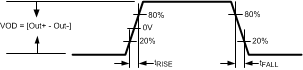 Figure 1. Output and Rise And Fall Transition Time
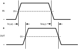 Figure 2. Propagation Delay Timing Diagram
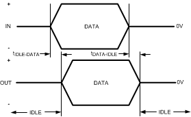 Figure 3. Transmit Idle-Data and Data-Idle Response Time
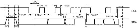 Figure 4. SMBus Timing Parameters
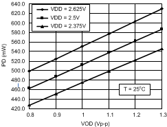
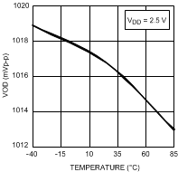
6.8 Typical Characteristics
7 Detailed Description
7.1 Overview
The DS125BR401A compensates for lossy FR-4 printed circuit board backplanes and balanced cables. The DS125BR401A operates in 3 modes: Terminal Control Mode (ENSMB = 0), SMBus Slave Mode (ENSMB = 1) and SMBus Master Mode (ENSMB = float) to load register information from external EEPROM; please refer to SMBus Master Mode for additional information.
7.2 Functional Block Diagram
B-Channel Datapath

A-Channel Datapath

7.2.1 Functional Datapath Blocks
The Channel-B datapath is designed to handle higher levels of input attenuation and includes an output with a soft-limiting function to provide some transparency for Rx-Tx training in SAS-3 and other standards. The Channel-A datapath has less input equalization coupled with a linear driver. This combination has a high level of transparency, achieving greater drive distance in SAS-3 applications which utilize Rx-Tx training. The asymmetrical channel design follows the application diagram in .
The Channel-A and Channel-B data-paths are optimized to work as a transparent driver and a transparent receiver. The typical DS125BR401A system placement breaks a long transmission line into two pieces. This often leads to one short and one long piece, this unequal partition places different demands on A and B-Channels. To maximize channel extension with the DS125BR401A, connect the A-Channel Inputs to the channel segment with the lowest attenuation to the SAS-3 Tx.
7.3 Feature Description
The 4-level input Terminals utilize a resistor divider to help set the 4 valid levels and provide a wider range of control settings when ENSMB=0. There is an internal 30K pull-up and a 60K pull-down connected to the package Terminal. These resistors, together with the external resistor connection combine to achieve the desired voltage level. Using the 1K pull-up, 1K pull-down, no connect, and 20K pull-down provide the optimal voltage levels for each of the four input states.
Table 1. 4–Level Control Terminal Settings
| Level | Setting | 3.3V Mode | 2.5V Mode |
|---|---|---|---|
| 0 | Tie 1kΩ to GND | 0.10 V | 0.08 V |
| R | Tie 20kΩ to GND | 1/3 x VIN | 1/3 x VDD |
| Float | Float (leave Terminal open) | 2/3 x VIN | 2/3 x VDD |
| 1 | Tie 1kΩ to VIN or VDD | VIN - 0.05 V | VDD - 0.04 V |
Typical 4-Level Input Thresholds
- Level 1 - 2 = 0.2 * VIN or VDD
- Level 2 - 3 = 0.5 * VIN or VDD
- Level 3 - 4 = 0.8 * VIN or VDD
In order to minimize the startup current associated with the integrated 2.5V regulator the 1K pull-up / pull-down resistors are recommended. If several 4 level inputs require the same setting, it is possible to combine two or more 1K resistors into a single lower value resistor. As an example; combining two inputs with a single 500 Ohm resistor is a good way to save board space.
7.4 Device Functional Modes
7.4.1 Terminal Control Mode:
When in Terminal mode (ENSMB = 0), equalization and de-emphasis can be selected via Terminal for each side independently. When de-emphasis is asserted VOD is automatically adjusted per Table 7. For PCIe applications, the RXDET Terminals provides automatic and manual control for input termination (50Ω or >50KΩ). MODE_B setting is also Terminal controllable with Terminal selections (Gen 1/2, auto detect, and SAS-3 / PCIe Gen 3). The receiver electrical signal detect threshold is also adjustable via the SD_TH Terminal. For A-Side Channels this can only be used for status information, on B-Side Channels this threshold will determine when the output state, Mute if no signal is present or active with a valid input signal detected .
7.4.2 SMBus Mode:
When in SMBus mode (ENSMB = 1), the VOD (output amplitude), equalization, de-emphasis, and termination disable features are all programmable on a individual lane basis, instead of grouped by A or B as in the Terminal mode case. Upon assertion of ENSMB, the EQx and DEMx functions revert to register control immediately. The EQx and DEMx Terminals are converted to AD0-AD3 SMBus address inputs. The other external control Terminals (MODE_B, RXDET and SD_TH) remain active unless their respective registers are written to and the appropriate override bit is set, in which case they are ignored until ENSMB is driven low (Terminal mode). On power-up or when ENSMB is driven low all registers are reset to their default state. If PWDN is asserted while ENSMB is high, the registers retain their current state.
Equalization settings accessible via the Terminal controls were chosen to meet the needs of most high speed applications. If additional fine tuning or adjustment is needed, additional equalization settings can be accessed via the SMBus registers. Each input has a total of 256 possible equalization settings. The tables show the 16 settings when the device is in Terminal mode. When using SMBus mode, the equalization, VOD and de- Emphasis levels are set by registers.
The 4-level input Terminals utilize a resistor divider to help set the 4 valid levels and provide a wider range of control settings when ENSMB=0. There is an internal 30K pull-up and a 60K pull-down connected to the package Terminal. These resistors, together with the external resistor connection combine to achieve the desired voltage level. Using the 1K pull-up, 1K pull-down, no connect, and 20K pull-down provide the optimal voltage levels for each of the four input states.
Table 2. RX-Detect Settings
| PWDN (Terminal 52) |
RXDET (Terminal 22) |
SMBus REG Bit[3:2] |
INPUT TERMINATION | RECOMMENDED USE | COMMENTS |
|---|---|---|---|---|---|
| 0 | 0 | 00 | Hi-Z | X | Manual RX-Detect, input is high impedance mode |
| 0 | Tie 20kΩ to GND |
01 | Pre Detect: Hi-Z Post Detect: 50 Ω |
PCIe only | Auto RX-Detect, outputs test every 12 msec for 600 msec then stops; termination is Hi-Z until RX detection; once detected input termination is 50 Ω Reset function by pulsing PWDN high for 5 usec then low again |
| 0 | Float (Default) |
10 | Pre Detect: Hi-Z Post Detect: 50 Ω |
PCIe only | Auto RX-Detect, outputs test every 12 msec until detection occurs; termination is Hi-Z until RX detection; once detected input termination is 50 Ω |
| 0 | 1 | 11 | 50 Ω | All Others | Manual RX-Detect, input is 50 Ω |
| 1 | X | High Impedance | X | Power down mode, input is Hi-Z, output drivers are disabled Used to reset RX-Detect State Machine when held high for 5 usec |
Table 3. OOB And Signal Detect Threshold Level(1)
| SD_TH (Terminal 26) |
SMBus REG BIT [3:2] and [1:0] | [3:2] ASSERT LEVEL (mVp-p) | [1:0] DE-ASSERT LEVEL (mVp-p) | ||
|---|---|---|---|---|---|
| 3 Gbps | 12 Gbps | 3 Gbps | 12 Gbps | ||
| 0 | 10 | 18 | 75 | 14 | 55 |
| R | 01 | 12 | 40 | 8 | 22 |
| F (default) | 00 | 15 | 50 | 11 | 37 |
| 1 | 11 | 16 | 58 | 12 | 45 |
Table 4. Mode Operation With Terminal Control
| MODE_B (Terminal 21) |
Driver characteristics | PCIe | SAS SATA |
10GbE | CPRI OBSAI |
SRIO (R)XAUI |
Interlaken Infiniband |
|---|---|---|---|---|---|---|---|
| 0 | Limiting | X (≤ 6G) | X | X | X | X | |
| R | Transparent without DE | ||||||
| F (default) | Automatic | X | |||||
| 1 | Transparent with DE | X (SAS-3) |
7.4.3 MODE operation with SMBus Registers
When in SMBus mode (Slave or Master), the MODE Terminal retains control of the output driver characteristics. In order to override this control function, Register 0x08[2] must be written with a "1". Writing this bit enables MODE control of each channel individually using the channel registers defined in Table 9. For Channel-A outputs the MODE control bit is not functional. The outputs are always in a linear mode of operation. Changing these bits while Register 0x08[2]=1 will dramatically reduce the output amplitude.
7.5 Signal Conditioning Settings
Information in Table 5 and Table 6 shows the level of CTLE or equalization gain for Channel-B and Channel-A.
Table 5. B-Channel Equalizer Settings
| Level | EQB1 | EQB0 | EQ – 8 bits [7:0] | dB at 1.5 GHz |
dB at 2.5 GHz |
dB at 4 GHz |
dB at 6 GHz |
Suggested Use(1) |
|---|---|---|---|---|---|---|---|---|
| 1 | 0 | 0 | 0000 0000 = 0x00 | 2.5 | 3.5 | 3.8 | 3.1 | FR4 < 5 inch trace |
| 2 | 0 | R | 0000 0001 = 0x01 | 3.8 | 5.4 | 6.7 | 6.7 | FR4 5-10 inch trace |
| 3 | 0 | Float | 0000 0010 = 0x02 | 5.0 | 7.0 | 8.4 | 8.4 | FR4 10 inch trace |
| 4 | 0 | 1 | 0000 0011 = 0x03 | 5.9 | 8.0 | 9.3 | 9.1 | FR4 15-20 inch trace |
| 5 | R | 0 | 0000 0111 = 0x07 | 7.4 | 10.3 | 12.8 | 13.7 | FR4 20-30 inch trace |
| 6 | R | R | 0001 0101 = 0x15 | 6.9 | 10.2 | 13.9 | 16.2 | FR4 25-30 inch trace |
| 7 | R | Float | 0000 1011 = 0x0B | 9.0 | 12.4 | 15.3 | 15.9 | FR4 25-30 inch trace |
| 8 | R | 1 | 0000 1111 = 0x0F | 10.2 | 13.8 | 16.7 | 17.0 | 8m, 30awg cable |
| 9 | Float | 0 | 0101 0101 = 0x55 | 8.5 | 12.6 | 17.5 | 20.7 | > 8m cable |
| 10 | Float | R | 0001 1111 = 0x1F | 11.7 | 16.2 | 20.3 | 21.8 | |
| 11 | Float | Float | 0010 1111 = 0x2F | 13.2 | 18.3 | 22.8 | 23.6 | |
| 12 | Float | 1 | 0011 1111 = 0x3F | 14.4 | 19.8 | 24.2 | 24.7 | |
| 13 | 1 | 0 | 1010 1010 = 0xAA | 14.4 | 20.5 | 26.4 | 28.0 | |
| 14 | 1 | R | 0111 1111 = 0x7F | 16.0 | 22.2 | 27.8 | 29.2 | |
| 15 | 1 | Float | 1011 1111 = 0xBF | 17.6 | 24.4 | 30.2 | 30.9 | |
| 16 | 1 | 1 | 1111 1111 = 0xFF | 18.7 | 25.8 | 31.6 | 31.9 |
Table 6. A-Channel Equalizer Settings
| Level | EQA1 | EQA0 | EQ – 8 bits [7:0] | dB at 1.5 GHz |
dB at 2.5 GHz |
dB at 4 GHz |
dB at 6 GHz |
Suggested Use(1) |
|---|---|---|---|---|---|---|---|---|
| 1 | N/A | 0 | xxxx xx00 = 0x00 | 2.5 | 3.5 | 3.8 | 3.1 | |
| 2 | N/A | R | xxxx xx01 = 0x01 | 3.8 | 5.4 | 6.7 | 6.7 | |
| 3 | N/A | Float | xxxx xx10 = 0x02 | 5.0 | 7.0 | 8.4 | 8.4 | |
| 4 | N/A | 1 | xxxx xx11 = 0x03 | 5.9 | 8.0 | 9.3 | 9.1 | SAS-3 |
Table 7. B-Channel Output Voltage And De-Emphasis Settings
| Level | DEMB1 | DEMB0 | VOD Vp-p | DEM dB(1) | Inner Amplitude Vp-p |
Suggested Use(2) |
|---|---|---|---|---|---|---|
| 1 | 0 | 0 | 0.8 | 0 | 0.8 | FR4 <5 inch trace |
| 2 | 0 | R | 0.9 | 0 | 0.9 | FR4 <5 inch trace |
| 3 | 0 | Float | 0.9 | - 3.5 | 0.6 | FR4 10 inch trace |
| 4 | 0 | 1 | 1.0 | 0 | 1.0 | FR4 <5 inch trace |
| 5 | R | 0 | 1.0 | - 3.5 | 0.7 | FR4 10 inch trace |
| 6 | R | R | 1.0 | - 6 | 0.5 | FR4 15 inch trace |
| 7 | R | Float | 1.1 | 0 | 1.1 | FR4 <5 inch trace |
| 8 | R | 1 | 1.1 | - 3.5 | 0.7 | FR4 10 inch trace |
| 9 | Float | 0 | 1.1 | - 6 | 0.6 | FR4 15 inch trace |
| 10 | Float | R | 1.2 | 0 | 1.2 | FR4 <5 inch trace |
| 11 | Float | Float | 1.2 | - 3.5 | 0.8 | FR4 10 inch trace |
| 12 | Float | 1 | 1.2 | - 6 | 0.6 | FR4 15 inch trace |
| 13 | 1 | 0 | 1.3 | 0 | 1.3 | FR4 <5 inch trace |
| 14 | 1 | R | 1.3 | - 3.5 | 0.9 | FR4 10 inch trace |
| 15 | 1 | Float | 1.3 | - 6 | 0.7 | FR4 15 inch trace |
| 16 | 1 | 1 | 1.3 | - 9 | 0.5 | FR4 20 inch trace |
Table 8. A-Channel Output Voltage And De-Emphasis Settings
| Level | DEMA1 | DEMA0 | VID Vp-p | DEM Setting(1) | VOD Vp-p |
|---|---|---|---|---|---|
| 1 | 0 | 0 | 1.0 | 0 | 0.70 |
| 2 | 0 | R | 1.0 | 0 | 0.78 |
| 4 | 0 | 1 | 1.0 | 0 | 0.83 |
| 7 | R | Float | 1.0 | 0 | 0.88 |
| 10 | Float | R | 1.0 | 0 | 0.91 |
| 13 | 1 | 0 | 1.0 | 0 | 1.00 |
7.6 Programming
The DS125BR401A device supports reading directly from an external EEPROM device by implementing SMBus Master mode. When using the SMBus master mode, the DS125BR401A will read directly from specific location in the external EEPROM. When designing a system for using the external EEPROM, the user needs to follow these specific guidelines.
- Maximum EEPROM size is 8 kbits (1024 x 8-bit).
- Set ENSMB = Float — enable the SMBus master mode.
- The external EEPROM device address byte must be 0xA0'h and capable of 400 kHz operation at 2.5V and 3.3V supply.
- Set the AD[3:0] inputs for SMBus address byte. When the AD[3:0] = 0000'b, the device address byte is B0'h.
When tying multiple DS125BR401A devices to the SDA and SCL bus, use these guidelines to configure the devices.
- Use SMBus AD[3:0] address bits so that each device can loaded it's configuration from the EEPROM. Example below is for 4 devices. The first device in the sequence must be address 0xB0'h, subsequent devices must follow the address order listed below.
- U1: AD[3:0] = 0000 = 0xB0'h,
- U2: AD[3:0] = 0001 = 0xB2'h,
- U3: AD[3:0] = 0010 = 0xB4'h,
- U4: AD[3:0] = 0011 = 0xB6'h
- Use a pull-up resistor on SDA and SCL; value = 2k ohms
- Daisy-chain READEN# (Terminal 26) and ALL_DONE# (Terminal 27) from one device to the next device in the sequence so that they do not compete for the EEPROM at the same time.
- Tie READEN# of the 1st device in the chain (U1) to GND
- Tie ALL_DONE# of U1 to READEN# of U2
- Tie ALL_DONE# of U2 to READEN# of U3
- Tie ALL_DONE# of U3 to READEN# of U4
- Optional: Tie ALL_DONE# output of U4 to a LED to show the devices have been loaded successfully
Below is an example of a 2 kbits (256 x 8-bit) EEPROM in hex format for the DS125BR401A device. The first 3 bytes of the EEPROM always contain a header common and necessary to control initialization of all devices connected to the I2C bus. CRC enable flag to enable/disable CRC checking. If CRC checking is disabled, a fixed pattern (8’hA5) is written/read instead of the CRC byte from the CRC location, to simplify the control. There is a MAP bit to flag the presence of an address map that specifies the configuration data start in the EEPROM. If the MAP bit is not present the configuration data start address is derived from the DS125BR401A address and the configuration data size. A bit to indicate an EEPROM size > 256 bytes is necessary to properly address the EEPROM. There are 37 bytes of data size for each DS125BR401A device.
:2000000000001000000407002FAD4002FAD4002FAD4002FAD409805F5A8005F5A8005F5AD0 :200020008005F5A800005454000000000000000000000000000000000000000000000000F6 :20006000000000000000000000000000000000000000000000000000000000000000000080 :20008000000000000000000000000000000000000000000000000000000000000000000060 :2000A000000000000000000000000000000000000000000000000000000000000000000040 :2000C000000000000000000000000000000000000000000000000000000000000000000020 :2000E000000000000000000000000000000000000000000000000000000000000000000000 :200040000000000000000000000000000000000000000000000000000000000000000000A0
Note: The maximum EEPROM size supported is 8 kbits (1024 x 8 bits).
Table 9. EEPROM Register Map - Single Device With Default Value
| EEPROM Address Byte | Bit 7 | Bit 6 | Bit 5 | Bit 4 | Bit 3 | Bit 2 | Bit 1 | BIt 0 | ||
|---|---|---|---|---|---|---|---|---|---|---|
| Description | 0 | CRC EN | Address Map Present | EEPROM > 256 Bytes | RES | DEVICE COUNT[3] | DEVICE COUNT[2] | DEVICE COUNT[1] | DEVICE COUNT[0] | |
| Value | 00 | 0 | 0 | 0 | 0 | 0 | 0 | 0 | 0 | |
| Description | 1 | RES | RES | RES | RES | RES | RES | RES | RES | |
| Value | 00 | 0 | 0 | 0 | 0 | 0 | 0 | 0 | 0 | |
| Description | 2 | Max EEPROM Burst size[7] | Max EEPROM Burst size[6] | Max EEPROM Burst size[5] | Max EEPROM Burst size[4] | Max EEPROM Burst size[3] | Max EEPROM Burst size[2] | Max EEPROM Burst size[1] | Max EEPROM Burst size[0] | |
| Value | 00 | 0 | 0 | 0 | 0 | 0 | 0 | 0 | 0 | |
| Description | 3 | PWDN_CH7 | PWDN_CH6 | PWDN_CH5 | PWDN_CH4 | PWDN_CH3 | PWDN_CH2 | PWDN_CH1 | PWDN_CH0 | |
| SMBus Register | 0x01 [7] | 0x01 [6] | 0x01 [5] | 0x01 [4] | 0x01 [3] | 0x01 [2] | 0x01 [1] | 0x01 [0] | ||
| Value | 00 | 0 | 0 | 0 | 0 | 0 | 0 | 0 | 0 | |
| Description | 4 | Reserved | Reserved | Reserved | Reserved | Ovrd_PWDN | CH7_EQ_LIM | CH6_EQ_LIM | CH5_EQ_LIM | |
| SMBus Register | 0x02 [5] | 0x02 [4] | 0x02 [3] | 0x02 [2] | 0x02 [0] | 0x04 [7] | 0x04 [6] | 0x04 [5] | ||
| Value | 00 | 0 | 0 | 0 | 0 | 0 | 0 | 0 | 0 | |
| Description | 5 | CH4_EQ_LIM | CH3_EQ_LIM | CH2_EQ_LIM | CH1_EQ_LIM | CH0_EQ_LIM | rxdet_btb_en | Ovrd_SD_TH | Reserved | |
| SMBus Register | 0x04 [4] | 0x04 [3] | 0x04 [2] | 0x04 [1] | 0x04 [0] | 0x06 [4] | 0x08 [6] | 0x08 [5] | ||
| Value | 04 | 0 | 0 | 0 | 0 | 0 | 1 | 0 | 0 | |
| Description | 6 | Ovrd_IDLE | Ovrd_RX_DET | Ovrd_MODE | Reserved | Reserved | rxdet_delay_2 | rxdet_delay_1 | rxdet_delay_0 | |
| SMBus Register | 0x08 [4] | 0x08 [3] | 0x08 [2] | 0x08 [1] | 0x08 [0] | 0x0B [6] | 0x0B [5] | 0x0B [4] | ||
| Value | 07 | 0 | 0 | 0 | 0 | 0 | 1 | 1 | 1 | |
| Description | 7 | rate_delay_3 | rate_delay_2 | rate_delay_1 | rate_delay_0 | CH0_Idle_auto | CH0_Idle_sel | CH0_Rxdet_1 | CH0_Rxdet_0 | |
| SMBus Register | 0x0B [3] | 0x0B [2] | 0x0B [1] | 0x0B [0] | 0x0E [5] | 0x0E [4] | 0x0E [3] | 0x0E [2] | ||
| Value | 00 | 0 | 0 | 0 | 0 | 0 | 0 | 0 | 0 | |
| Description | 8 | CH0_EQ_7 | CH0_EQ_6 | CH0_EQ_5 | CH0_EQ_4 | CH0_EQ_3 | CH0_EQ_2 | CH0_EQ_1 | CH0_EQ_0 | |
| SMBus Register | 0x0F [7] | 0x0F [6] | 0x0F [5] | 0x0F [4] | 0x0F [3] | 0x0F [2] | 0x0F [1] | 0x0F [0] | ||
| Value | 2F | 0 | 0 | 1 | 0 | 1 | 1 | 1 | 1 | |
| Description | 9 | CH0_SCP | CH0_MODE | Reserved | Reserved | Reserved | CH0_VOD_2 | CH0_VOD_1 | CH0_VOD_0 | |
| SMBus Register | 0x10 [7] | 0x10 [6] | 0x10 [5] | 0x10 [4] | 0x10 [3] | 0x10 [2] | 0x10 [1] | 0x10 [0] | ||
| Value | AD | 1 | 0 | 1 | 0 | 1 | 1 | 0 | 1 | |
| Description | A | CH0_DEM_2 | CH0_DEM_1 | CH0_DEM_0 | Reserved | CH0_THa_1 | CH0_THa_0 | CH0_THd_1 | CH0_THd_0 | |
| SMBus Register | 0x11 [2] | 0x11 [1] | 0x11 [0] | 0x12 [7] | 0x12 [3] | 0x12 [2] | 0x12 [1] | 0x12 [0] | ||
| Value | 40 | 0 | 1 | 0 | 0 | 0 | 0 | 0 | 0 | |
| Description | B | CH1_Idle_auto | CH1_Idle_sel | CH1_Rxdet_1 | CH1_Rxdet_0 | CH1_EQ_7 | CH1_EQ_6 | CH1_EQ_5 | CH1_EQ_4 | |
| SMBus Register | 0x15 [5] | 0x15 [4] | 0x15 [3] | 0x15 [2] | 0x16 [7] | 0x16 [6] | 0x16 [5] | 0x16 [4] | ||
| Value | 02 | 0 | 0 | 0 | 0 | 0 | 0 | 1 | 0 | |
| Description | C | CH1_EQ_3 | CH1_EQ_2 | CH1_EQ_1 | CH1_EQ_0 | CH1_SCP | CH1_MODE | Reserved | Reserved | |
| SMBus Register | 0x16 [3] | 0x16 [2] | 0x16 [1] | 0x16 [0] | 0x17 [7] | 0x17 [6] | 0x17 [5] | 0x17 [4] | ||
| Value | FA | 1 | 1 | 1 | 1 | 1 | 0 | 1 | 0 | |
| Description | D | Reserved | CH1_VOD_2 | CH1_VOD_1 | CH1_VOD_0 | CH1_DEM_2 | CH1_DEM_1 | CH1_DEM_0 | Reserved | |
| SMBus Register | 0x17 [3] | 0x17 [2] | 0x17 [1] | 0x17 [0] | 0x18 [2] | 0x18 [1] | 0x18 [0] | 0x19 [7] | ||
| Value | D4 | 1 | 1 | 0 | 1 | 0 | 1 | 0 | 0 | |
| Description | E | CH1_THa_1 | CH1_THa_0 | CH1_THd_1 | CH1_THd_0 | CH2_Idle_auto | CH2_Idle_sel | CH2_Rxdet_1 | CH2_Rxdet_0 | |
| SMBus Register | 0x19 [3] | 0x19 [2] | 0x19 [1] | 0x19 [0] | 0x1C [5] | 0x1C [4] | 0x1C [3] | 0x1C [2] | ||
| Value | 00 | 0 | 0 | 0 | 0 | 0 | 0 | 0 | 0 | |
| Description | F | CH2_EQ_7 | CH2_EQ_6 | CH2_EQ_5 | CH2_EQ_4 | CH2_EQ_3 | CH2_EQ_2 | CH2_EQ_1 | CH2_EQ_0 | |
| SMBus Register | 0x1D [7] | 0x1D [6] | 0x1D [5] | 0x1D [4] | 0x1D [3] | 0x1D [2] | 0x1D [1] | 0x1D [0] | ||
| Value | 2F | 0 | 0 | 1 | 0 | 1 | 1 | 1 | 1 | |
| Description | 10 | CH2_SCP | CH2_MODE | Reserved | Reserved | Reserved | CH2_VOD_2 | CH2_VOD_1 | CH2_VOD_0 | |
| SMBus Register | 0x1E [7] | 0x1E [6] | 0x1E [5] | 0x1E [4] | 0x1E [3] | 0x1E [2] | 0x1E [1] | 0x1E [0] | ||
| Value | AD | 1 | 0 | 1 | 0 | 1 | 1 | 0 | 1 | |
| Description | 11 | CH2_DEM_2 | CH2_DEM_1 | CH2_DEM_0 | Reserved | CH2_THa_1 | CH2_THa_0 | CH2_THd_1 | CH2_THd_0 | |
| SMBus Register | 0x1F [2] | 0x1F [1] | 0x1F [0] | 0x20 [7] | 0x20 [3] | 0x20 [2] | 0x20 [1] | 0x20 [0] | ||
| Value | 40 | 0 | 1 | 0 | 0 | 0 | 0 | 0 | 0 | |
| Description | 12 | CH3_Idle_auto | CH3_Idle_sel | CH3_Rxdet_1 | CH3_Rxdet_0 | CH3_EQ_7 | CH3_EQ_6 | CH3_EQ_5 | CH3_EQ_4 | |
| SMBus Register | 0x23 [5] | 0x23 [4] | 0x23 [3] | 0x23 [2] | 0x24 [7] | 0x24 [6] | 0x24 [5] | 0x24 [4] | ||
| Value | 02 | 0 | 0 | 0 | 0 | 0 | 0 | 1 | 0 | |
| Description | 13 | CH3_EQ_3 | CH3_EQ_2 | CH3_EQ_1 | CH3_EQ_0 | CH3_SCP | CH3_MODE | Reserved | Reserved | |
| SMBus Register | 0x24 [3] | 0x24 [2] | 0x24 [1] | 0x24 [0] | 0x25 [7] | 0x25 [6] | 0x25 [5] | 0x25 [4] | ||
| Value | FA | 1 | 1 | 1 | 1 | 1 | 0 | 1 | 0 | |
| Description | 14 | Reserved | CH3_VOD_2 | CH3_VOD_1 | CH3_VOD_0 | CH3_DEM_2 | CH3_DEM_1 | CH3_DEM_0 | Reserved | |
| SMBus Register | 0x25 [3] | 0x25 [2] | 0x25 [1] | 0x25 [0] | 0x26 [2] | 0x26 [1] | 0x26 [0] | 0x27 [7] | ||
| Value | D4 | 1 | 1 | 0 | 1 | 0 | 1 | 0 | 0 | |
| Description | 15 | CH3_THa_1 | CH3_THa_0 | CH3_THd_1 | CH3_THd_0 | ovrd_fast_idle | hi_idle_th CH0-3 | hi_idle_thCH4-7 | fast_idle CH0-3 | |
| SMBus Register | 0x27 [3] | 0x27 [2] | 0x27 [1] | 0x27 [0] | 0x28 [6] | 0x28 [5] | 0x28 [4] | 0x28 [3] | ||
| Value | 09 | 0 | 0 | 0 | 0 | 1 | 0 | 0 | 1 | |
| Description | 16 | fast_idle CH4-7 | low_gain CH0-3 | low_gain CH4-7 | CH4_Idle_auto | CH4_Idle_sel | CH4_Rxdet_1 | CH4_Rxdet_0 | Reserved | |
| SMBus Register | 0x28 [2] | 0x28 [1] | 0x28 [0] | 0x2B [5] | 0x2B [4] | 0x2B [3] | 0x2B [2] | 0x2C [7] | ||
| Value | 80 | 1 | 0 | 0 | 0 | 0 | 0 | 0 | 0 | |
| Description | 17 | Reserved | Reserved | Reserved | Reserved | Reserved | CH4_EQ_1 | CH4_EQ_0 | CH4_SCP | |
| SMBus Register | 0x2C [6] | 0x2C [5] | 0x2C [4] | 0x2C [3] | 0x2C [2] | 0x2C [1] | 0x2C [0] | 0x2D [7] | ||
| Value | 5F | 0 | 1 | 0 | 1 | 1 | 1 | 1 | 1 | |
| Description | 18 | Reserved | Reserved | Reserved | Reserved | CH4_VOD_2 | CH4_VOD_1 | CH4_VOD_0 | CH4_DEM_2 | |
| SMBus Register | 0x2D [6] | 0x2D [5] | 0x2D [4] | 0x2D [3] | 0x2D [2] | 0x2D [1] | 0x2D [0] | 0x2E [2] | ||
| Value | 5A | 0 | 1 | 0 | 1 | 1 | 0 | 1 | 0 | |
| Description | 19 | CH4_DEM_1 | CH4_DEM_0 | Reserved | CH4_THa_1 | CH4_THa_0 | CH4_THd_1 | CH4_THd_0 | CH5_Idle_auto | |
| SMBus Register | 0x2E [1] | 0x2E [0] | 0x2F [7] | 0x2F [3] | 0x2F [2] | 0x2F [1] | 0x2F [0] | 0x32 [5] | ||
| Value | 80 | 1 | 0 | 0 | 0 | 0 | 0 | 0 | 0 | |
| Description | 1A | CH5_Idle_sel | CH5_Rxdet_1 | CH5_Rxdet_0 | Reserved | Reserved | Reserved | Reserved | Reserved | |
| SMBus Register | 0x32 [4] | 0x32 [3] | 0x32 [2] | 0x33 [7] | 0x33 [6] | 0x33 [5] | 0x33 [4] | 0x33 [3] | ||
| Value | 05 | 0 | 0 | 0 | 0 | 0 | 1 | 0 | 1 | |
| Description | 1B | Reserved | CH5_EQ_1 | CH5_EQ_0 | CH5_SCP | Reserved | Reserved | Reserved | Reserved | |
| SMBus Register | 0x33 [2] | 0x33 [1] | 0x33 [0] | 0x34 [7] | 0x34 [6] | 0x34 [5] | 0x34 [4] | 0x34 [3] | ||
| Value | F5 | 1 | 1 | 1 | 1 | 0 | 1 | 0 | 1 | |
| Description | 1C | CH5_VOD_2 | CH5_VOD_1 | CH5_VOD_0 | CH5_DEM_2 | CH5_DEM_1 | CH5_DEM_0 | Reserved | CH5_THa_1 | |
| SMBus Register | 0x34 [2] | 0x34 [1] | 0x34 [0] | 0x35 [2] | 0x35 [1] | 0x35 [0] | 0x36 [7] | 0x36 [3] | ||
| Value | A8 | 1 | 0 | 1 | 0 | 1 | 0 | 0 | 0 | |
| Description | 1D | CH5_THa_0 | CH5_THd_1 | CH5_THd_0 | CH6_Idle_auto | CH6_Idle_sel | CH6_Rxdet_1 | CH6_Rxdet_0 | Reserved | |
| SMBus Register | 0x36 [2] | 0x36 [1] | 0x36 [0] | 0x39 [5] | 0x39 [4] | 0x39 [3] | 0x39 [2] | 0x3A [7] | ||
| Value | 00 | 0 | 0 | 0 | 0 | 0 | 0 | 0 | 0 | |
| Description | 1E | Reserved | Reserved | Reserved | Reserved | Reserved | CH6_EQ_1 | CH6_EQ_0 | CH6_SCP | |
| SMBus Register | 0x3A [6] | 0x3A [5] | 0x3A [4] | 0x3A [3] | 0x3A [2] | 0x3A [1] | 0x3A [0] | 0x3B [7] | ||
| Value | 5F | 0 | 1 | 0 | 1 | 1 | 1 | 1 | 1 | |
| Description | 1F | Reserved | Reserved | Reserved | Reserved | CH6_VOD_2 | CH6_VOD_1 | CH6_VOD_0 | CH6_DEM_2 | |
| SMBus Register | 0x3B [6] | 0x3B [5] | 0x3B [4] | 0x3B [3] | 0x3B [2] | 0x3B [1] | 0x3B [0] | 0x3C [2] | ||
| Value | 5A | 0 | 1 | 0 | 1 | 1 | 0 | 1 | 0 | |
| Description | 20 | CH6_DEM_1 | CH6_DEM_0 | Reserved | CH6_THa_1 | CH6_THa_0 | CH6_THd_1 | CH6_THd_0 | CH7_Idle_auto | |
| SMBus Register | 0x3C [1] | 0x3C [0] | 0x3D [7] | 0x3D [3] | 0x3D [2] | 0x3D [1] | 0x3D [0] | 0x40 [5] | ||
| Value | 80 | 1 | 0 | 0 | 0 | 0 | 0 | 0 | 0 | |
| Description | 21 | CH7_Idle_sel | CH7_Rxdet_1 | CH7_Rxdet_0 | Reserved | Reserved | Reserved | Reserved | Reserved | |
| SMBus Register | 0x40 [4] | 0x40 [3] | 0x40 [2] | 0x41 [7] | 0x41 [6] | 0x41 [5] | 0x41 [4] | 0x41 [3] | ||
| Value | 05 | 0 | 0 | 0 | 0 | 0 | 1 | 0 | 1 | |
| Description | 22 | Reserved | CH7_EQ_1 | CH7_EQ_0 | CH7_SCP | Reserved | Reserved | Reserved | Reserved | |
| SMBus Register | 0x41 [2] | 0x41 [1] | 0x41 [0] | 0x42 [7] | 0x42 [6] | 0x42 [5] | 0x42 [4] | 0x42 [3] | ||
| Value | F5 | 1 | 1 | 1 | 1 | 0 | 1 | 0 | 1 | |
| Description | 23 | CH7_VOD_2 | CH7_VOD_1 | CH7_VOD_0 | CH7_DEM_2 | CH7_DEM_1 | CH7_DEM_0 | Reserved | CH7_THa_1 | |
| SMBus Register | 0x42 [2] | 0x42 [1] | 0x42 [0] | 0x43 [2] | 0x43 [1] | 0x43 [0] | 0x44 [7] | 0x44 [3] | ||
| Value | A8 | 1 | 0 | 1 | 0 | 1 | 0 | 0 | 0 | |
| Description | 24 | CH7_THa_0 | CH7_THd_1 | CH7_THd_0 | Reserved | Reserved | Reserved | Reserved | Reserved | |
| SMBus Register | 0x44 [2] | 0x44 [1] | 0x44 [0] | 0x47 [3] | 0x47 [2] | 0x47 [2] | 0x47 [0] | 0x48 [7] | ||
| Value | 00 | 0 | 0 | 0 | 0 | 0 | 0 | 0 | 0 | |
| Description | 25 | Reserved | Reserved | Reserved | Reserved | Reserved | Reserved | Reserved | Reserved | |
| SMBus Register | 0x48 [6] | 0x4C [7] | 0x4C [6] | 0x4C [5] | 0x4C [4] | 0x4C [3] | 0x4C [0] | 0x59 [0] | ||
| Value | 00 | 0 | 0 | 0 | 0 | 0 | 0 | 0 | 0 | |
| Description | 26 | Reserved | Reserved | Reserved | Reserved | Reserved | Reserved | Reserved | Reserved | |
| SMBus Register | 0x5A [7] | 0x5A [6] | 0x5A [5] | 0x5A [4] | 0x5A [3] | 0x5A [2] | 0x5A [1] | 0x5A [0] | ||
| Value | 54 | 0 | 1 | 0 | 1 | 0 | 1 | 0 | 0 | |
| Description | 27 | Reserved | Reserved | Reserved | Reserved | Reserved | Reserved | Reserved | Reserved | |
| SMBus Register | 0x5B [7] | 0x5B [6] | 0x5B [5] | 0x5B [4] | 0x5B [3] | 0x5B [2] | 0x5B [1] | 0x5B [0] | ||
| Value | 54 | 0 | 1 | 0 | 1 | 0 | 1 | 0 | 0 | |
Table 10. Example Of EEPROM For Four Devices Using Two Address Maps
| EEPROM Address | Address (Hex) | EEPROM Data | Comments |
|---|---|---|---|
| 0 | 00 | 0x43 | CRC_EN = 0, Address Map = 1, >256 bytes = 0, Device Count[3:0] = 3 |
| 1 | 01 | 0x00 | |
| 2 | 02 | 0x08 | EEPROM Burst Size |
| 3 | 03 | 0x00 | CRC not used |
| 4 | 04 | 0x0B | Device 0 Address Location |
| 5 | 05 | 0x00 | CRC not used |
| 6 | 06 | 0x0B | Device 1 Address Location |
| 7 | 07 | 0x00 | CRC not used |
| 8 | 08 | 0x30 | Device 2 Address Location |
| 9 | 09 | 0x00 | CRC not used |
| 10 | 0A | 0x30 | Device 3 Address Location |
| 11 | 0B | 0x00 | Begin Device 0, 1 - Address Offset 3 |
| 12 | 0C | 0x00 | |
| 13 | 0D | 0x04 | |
| 14 | 0E | 0x07 | |
| 15 | 0F | 0x00 | |
| 16 | 10 | 0x01 | EQ CHB0 = 01 |
| 17 | 11 | 0xAD | VOD CHB0 = 1.2V |
| 18 | 12 | 0x00 | DEM CHB0 = 0 (0dB) |
| 19 | 13 | 0x00 | EQ CHB1 = 01 |
| 20 | 14 | 0x1A | VOD CHB1 = 1.2V |
| 21 | 15 | 0xD0 | DEM CHB1 = 0 (0dB) |
| 22 | 16 | 0x00 | |
| 23 | 17 | 0x01 | EQ CHB2 = 01 |
| 24 | 18 | 0xAD | VOD CHB2 = 1.2V |
| 25 | 19 | 0x00 | DEM CHB2 = 0 (0dB) |
| 26 | 1A | 0x00 | EQ CHB3 = 01 |
| 27 | 1B | 0x1A | VOD CHB3 = 1.2V |
| 28 | 1C | 0xD0 | DEM CHB3 = 0 (0dB) |
| 29 | 1D | 0x09 | Signal Detect Control |
| 30 | 1E | 0x80 | Signal Detect Control |
| 31 | 1F | 0x07 | EQ CHA0 = 03 |
| 32 | 20 | 0x5E | VOD CHA0 = 111'b |
| 33 | 21 | 0x00 | DEM CHA0 = 0 (0dB) |
| 34 | 22 | 0x00 | EQ CHA1 = 03 |
| 35 | 23 | 0x75 | VOD CHA1 = 111'b |
| 36 | 24 | 0xE0 | DEM CHA1 = 0 (0dB) |
| 37 | 25 | 0x00 | |
| 38 | 26 | 0x07 | EQ CHA2 = 03 |
| 39 | 27 | 0x5E | VOD CHA2 = 1.4V |
| 40 | 28 | 0x00 | DEM CHA2 = 0 (0dB) |
| 41 | 29 | 0x00 | EQ CHA3 = 03 |
| 42 | 2A | 0x75 | VOD CHA3 = 111'b |
| 43 | 2B | 0xE0 | DEM CHA3 = 0 (0dB) |
| 44 | 2C | 0x00 | |
| 45 | 2D | 0x00 | |
| 46 | 2E | 0x54 | |
| 47 | 2F | 0x54 | End Device 0, 1 - Address Offset 39 |
| 48 | 30 | 0x00 | Begin Device 2, 3 - Address Offset 3 |
| 49 | 31 | 0x00 | |
| 50 | 32 | 0x04 | |
| 51 | 33 | 0x07 | |
| 52 | 34 | 0x00 | |
| 53 | 35 | 0x01 | EQ CHB0 = 01 |
| 54 | 36 | 0xAB | VOD CHB0 = 1.0V |
| 55 | 37 | 0x00 | DEM CHB0 = 0 (0dB) |
| 56 | 38 | 0x00 | EQ CHB1 = 01 |
| 57 | 39 | 0x1A | VOD CHB1 = 1.0V |
| 58 | 3A | 0xB0 | DEM CHB1 = 0 (0dB) |
| 59 | 3B | 0x00 | |
| 60 | 3C | 0x01 | EQ CHB2 = 01 |
| 61 | 3D | 0xAB | VOD CHB2 = 1.0V |
| 62 | 3E | 0x00 | DEM CHB2 = 0 (0dB) |
| 63 | 3F | 0x00 | EQ CHB3 = 01 |
| 64 | 40 | 0x1A | VOD CHB3 = 1.0V |
| 65 | 41 | 0xB0 | DEM CHB3 = 0 (0dB) |
| 66 | 42 | 0x09 | Signal Detect Control |
| 67 | 43 | 0x80 | Signal Detect Control |
| 68 | 44 | 0x03 | EQ CHA0 = 01 |
| 69 | 45 | 0x5E | VOD CHA0 = 111'b |
| 70 | 46 | 0x00 | DEM CHA0 = 0 (0dB) |
| 71 | 47 | 0x00 | EQ CHA1 = 01 |
| 72 | 48 | 0x35 | VOD CHA1 = 111'b |
| 73 | 49 | 0xE0 | DEM CHA1 = 0 (0dB) |
| 74 | 4A | 0x00 | |
| 75 | 4B | 0x03 | EQ CHA2 = 01 |
| 76 | 4C | 0x5E | VOD CHA2 = 111'b |
| 77 | 4D | 0x00 | DEM CHA2 = 0 (0dB) |
| 78 | 4E | 0x00 | EQ CHA3 = 01 |
| 79 | 4F | 0x35 | VOD CHA3 = 111'b |
| 80 | 50 | 0xE0 | DEM CHA3 = 0 (0dB) |
| 81 | 51 | 0x00 | |
| 82 | 52 | 0x00 | |
| 83 | 53 | 0x54 | |
| 84 | 54 | 0x54 | End Device 2, 3 - Address Offset 39 |
Note: CRC_EN = 0, Address Map = 1, >256 byte = 0, Device Count[3:0] = 3. Multiple devices can point to the same address map. Maximum EEPROM size is 8 kbits (1024 x 8-bits).
7.7 Register Maps
The System Management Bus interface is compatible to SMBus 2.0 physical layer specification. ENSMB = 1kΩ to VDD to enable SMBus slave mode and allow access to the configuration registers.
The DS125BR401A has the AD[3:0] inputs in SMBus mode. These Terminals are the user set SMBus slave address inputs. The AD[3:0] Terminals have internal pull-down. When left floating or pulled low the AD[3:0] = 0000'b, the device default address byte is B0'h. Based on the SMBus 2.0 specification, the DS125BR401A has a 7-bit slave address. The LSB is set to 0'b (for a WRITE). The device supports up to 16 address byte, which can be set with the AD[3:0] inputs. Below are the 16 addresses.
Table 11. Device Slave Address Bytes
| AD[3:0] Settings | Address Bytes (HEX) |
|---|---|
| 0000 | B0 |
| 0001 | B2 |
| 0010 | B4 |
| 0011 | B6 |
| 0100 | B8 |
| 0101 | BA |
| 0110 | BC |
| 0111 | BE |
| 1000 | C0 |
| 1001 | C2 |
| 1010 | C4 |
| 1011 | C6 |
| 1100 | C8 |
| 1101 | CA |
| 1110 | CC |
| 1111 | CE |
The SDA, SCL Terminals are 3.3V tolerant, but are not 5V tolerant. External pull-up resistor is required on the SDA. The resistor value can be from 1 kΩ to 5 kΩ depending on the voltage, loading and speed. The SCL may also require an external pull-up resistor and it depends on the Host that drives the bus.
7.7.1 Transfer Of Data Via The SMBus
During normal operation the data on SDA must be stable during the time when SCL is High.
There are three unique states for the SMBus:
START: A High-to-Low transition on SDA while SCL is High indicates a message START condition.
STOP: A Low-to-High transition on SDA while SCL is High indicates a message STOP condition.
IDLE: If SCL and SDA are both High for a time exceeding tBUF from the last detected STOP condition or if they are High for a total exceeding the maximum specification for tHIGH then the bus will transfer to the IDLE state.
7.7.2 SMBus Transactions
The device supports WRITE and READ transactions. See Table 12 for register address, type (Read/Write, Read Only), default value and function information.
7.7.3 Writing a Register
To write a register, the following protocol is used (see SMBus 2.0 specification).
- The Host drives a START condition, the 7-bit SMBus address, and a “0” indicating a WRITE.
- The Device (Slave) drives the ACK bit (“0”).
- The Host drives the 8-bit Register Address.
- The Device drives an ACK bit (“0”).
- The Host drive the 8-bit data byte.
- The Device drives an ACK bit (“0”).
- The Host drives a STOP condition.
The WRITE transaction is completed, the bus goes IDLE and communication with other SMBus devices may now occur.
7.7.4 Reading a Register
To read a register, the following protocol is used (see SMBus 2.0 specification).
- The Host drives a START condition, the 7-bit SMBus address, and a “0” indicating a WRITE.
- The Device (Slave) drives the ACK bit (“0”).
- The Host drives the 8-bit Register Address.
- The Device drives an ACK bit (“0”).
- The Host drives a START condition.
- The Host drives the 7-bit SMBus Address, and a “1” indicating a READ.
- The Device drives an ACK bit “0”.
- The Device drives the 8-bit data value (register contents).
- The Host drives a NACK bit “1”indicating end of the READ transfer.
- The Host drives a STOP condition.
The READ transaction is completed, the bus goes IDLE and communication with other SMBus devices may now occur.
Table 12 for more information.
Table 12. SMBus Slave Mode Register Map
| Address | Register Name | Bit | Field | Type | Default | Description |
|---|---|---|---|---|---|---|
| 0x00 | Observation | 7 | Reserved | R/W | 0x00 | Set bit to 0. |
| 6:3 | Address Bit AD[3:0] |
R | Observation of AD[3:0] bits [6]: AD3 [5]: AD2 [4]: AD1 [3]: AD0 |
|||
| 2 | EEPROM Read Done | R | 1: Device completed the read from external EEPROM. | |||
| 1 | Reserved | R/W | Set bit to 0. | |||
| 0 | Reserved | R/W | Set bit to 0. | |||
| 0x01 | PWDN Channels | 7:0 | PWDN CHx | R/W | 0x00 | Power Down per Channel [7]: CH7 – CHA_3 [6]: CH6 – CHA_2 [5]: CH5 – CHA_1 [4]: CH4 – CHA_0 [3]: CH3 – CHB_3 [2]: CH2 – CHB_2 [1]: CH1 – CHB_1 [0]: CH0 – CHB_0 00'h = all channels enabled FF'h = all channels disabled Note: override PWDN Terminal. |
| 0x02 | Override PWDN | 7:1 | Reserved | R/W | 0x00 | Set bits to 0. |
| 0 | Override PWDN Terminal |
1: Block PWDN Terminal control 0: Allow PWDN Terminal control |
||||
| 0x04 | EQ Limiting | 7:0 | EQ Control | R/W | 0x00 | CH3 - CH0 EQ Limiting Control [7]: CH7 – CHA_3 (linear only) [6]: CH6 – CHA_2 (linear only) [5]: CH5 – CHA_1 (linear only) [4]: CH4 – CHA_0 (linear only) [3]: CH3 – CHB_3 [2]: CH2 – CHB_2 [1]: CH1 – CHB_1 [0]: CH0 – CHB_0 00'h = all channels linear EQ 0F'h = B-channels limiting EQ Note: These bits do not connect to the A-Channel |
| 0x05 | Slave Mode CRC bits | 7:0 | CRC bits | R/W | 0x00 | CRC bits [7:0] |
| 0x06 | Slave Register Control | 7:5 | Reserved | R/W | 0x10 | Set bits to 0. |
| 4 | Reserved | Set bit to 1. | ||||
| 3 | Register Enable | 1: Enables high speed channel control via SMBus registers without CRC 0: Channel control via SMBus registers requires correct CRC in Reg 0x05 Note: In order to change VOD, DEM and EQ of the channels in slave mode without also setting CRC each time, set this bit to 1. |
||||
| 2:0 | Reserved | Set bits to 0. | ||||
| 0x07 | Digital Reset and Control | 7 | Reserved | R/W | 0x01 | Set bit to 0. |
| 6 | Reset Registers | Self clearing reset for SMBus registers. Writing a [1] will return register settings to default values. | ||||
| 5 | Reset SMBus Master | Self clearing reset to SMBus master state machine | ||||
| 4:0 | Reserved | Set bits to 0 0001'b. | ||||
| 0x08 | Override Terminal Control |
7 | Reserved | R/W | 0x00 | Set bit to 0. |
| 6 | Override SD_TH | 1: Block SD_TH Terminal control 0: Allow SD_TH Terminal control |
||||
| 5 | Reserved | Set bit to 0. | ||||
| 4 | Override IDLE | 1: IDLE control by registers 0: IDLE control by signal detect Note: These bits do not connect to the A-Channel |
||||
| 3 | Override RXDET | 1: Block RXDET Terminal control 0: Allow RXDET Terminal control |
||||
| 2 | Override MODE_B | 1: Block MODE_B Terminal control 0: Allow MODE_B Terminal control |
||||
| 1 | Reserved | Set bit to 0. | ||||
| 0 | Reserved | Set bit to 0. | ||||
| 0x0A | Signal Detect Monitor | 7:0 | IDLE Status | R | 0x00 | CH7 - CH0 Internal IDLE indicator [7]: CH7 – CHA_3 [6]: CH6 – CHA_2 [5]: CH5 – CHA_1 [4]: CH4 – CHA_0 [3]: CH3 – CHB_3 [2]: CH2 – CHB_2 [1]: CH1 – CHB_1 [0]: CH0 – CHB_0 0'b = Signal Detected at input 1'b = Signal Detected at input Note: These bits only function when MODE_B terminal = FLOAT |
| 0x0E | CH0 - CHB0 IDLE, RXDET |
7:6 | Reserved | R/W | 0x00 | Set bits to 0. |
| 5 | IDLE_AUTO | 1: Automatic IDLE detect 0: Allow IDLE_SEL control in bit 4 Note: override IDLE control. |
||||
| 4 | IDLE_SEL | 1: Output is MUTED (electrical idle) 0: Output is ON Note: override IDLE control. |
||||
| 3:2 | RXDET | 00: Input is high-z impedance 01: Auto RX-Detect, outputs test every 12 ms for 600 ms (50 times) then stops; termination is high-z until detection; once detected input termination is 50 Ω 10: Auto RX-Detect, outputs test every 12 ms until detection occurs; termination is high-z until detection; once detected input termination is 50 Ω 11: Input is 50 Ω Note: override RXDET Terminal. |
||||
| 1:0 | Reserved | Set bits to 0. | ||||
| 0x0F | CH0 - CHB0 EQ |
7:0 | EQ Control | R/W | 0x2F | INB_0 EQ Control - total of 256 levels. See Table 5. |
| 0x10 | CH0 - CHB_0 VOD |
7 | Short Circuit Protection | R/W | 0xAD | 1: Enable the short circuit protection 0: Disable the short circuit protection |
| 6 | MODE_SEL | 1: PCIe Gen 1/2 0: SAS-3 and PCIe Gen 3 Note: override the MODE_B Terminal. |
||||
| 5:3 | Reserved | Set bits to default value - 101. | ||||
| 2:0 | VOD Control | OUTB_0 VOD Control 000: 0.7 V 001: 0.8 V 010: 0.9 V 011: 1.0 V 100: 1.1 V 101: 1.2 V (default) 110: 1.3 V 111: 1.4 V |
||||
| 0x11 | CH0 - CHB_0 DEM |
7 | RXDET STATUS | R | 0x02 | Observation bit for RXDET CH0 - CHB_0. 1: RX = detected 0: RX = not detected |
| 6:5 | MODE_DET STATUS | R | Observation bit for MODE_DET CH0 - CHB_0. 00: GEN1 (2.5G data-rate) 01: GEN2 (5G data-rate) 11: GEN3 (8G+ data-rate) Note: Only functions when MODE_B Terminal = Automatic |
|||
| 4:3 | Reserved | R/W | Set bits to 0. | |||
| 2:0 | DEM Control | R/W | OUTB_0 DEM Control 000: 0 dB 001: –1.5 dB 010: –3.5 dB (default) 011: –5 dB 100: –6 dB 101: –8 dB 110: –9 dB 111: –12 dB |
|||
| 0x12 | CH0 - CHB_0 SD Threshold |
7:4 | Reserved | R/W | 0x00 | Set bits to 0. |
| 3:2 | IDLE tha | Assert threshold (1010 pattern 12 Gbps) 00 = 50 mVp-p (default) 01 = 40 mVp-p 10 = 75 mVp-p 11 = 58 mVp-p Note: override the SD_TH Terminal using 0x08[6]. |
||||
| 1:0 | IDLE thd | De-assert threshold (1010 pattern 12 Gbps) 00 = 37 mVp-p (default) 01 = 22 mVp-p 10 = 55 mVp-p 11 = 45 mVp-p Note: override the SD_TH Terminal using 0x08[6]. |
||||
| 0x15 | CH1 - CHB_1 IDLE, RXDET |
7:6 | Reserved | R/W | 0x00 | Set bits to 0. |
| 5 | IDLE_AUTO | 1: Automatic IDLE detect 0: Allow IDLE_SEL control in bit 4 Note: override IDLE control. |
||||
| 4 | IDLE_SEL | 1: Output is MUTED (electrical idle) 0: Output is ON Note: override IDLE control. |
||||
| 3:2 | RXDET | 00: Input is high-z impedance 01: Auto RX-Detect, outputs test every 12 ms for 600 ms (50 times) then stops; termination is high-z until detection; once detected input termination is 50 Ω 10: Auto RX-Detect, outputs test every 12 ms until detection occurs; termination is high-z until detection; once detected input termination is 50 Ω 11: Input is 50 Ω Note: override RXDET Terminal. |
||||
| 1:0 | Reserved | Set bits to 0. | ||||
| 0x16 | CH1 - CHB_1 EQ |
7:0 | EQ Control | R/W | 0x2F | INB_1 EQ Control - total of 256 levels. See Table 5. |
| 0x17 | CH1 - CHB_1 VOD |
7 | Short Circuit Protection | R/W | 0xAD | 1: Enable the short circuit protection 0: Disable the short circuit protection |
| 6 | MODE_SEL | 1: Gen 1/2, 0: SAS-3 and PCIe Gen 3 Note: override the MODE_B Terminal. |
||||
| 5:3 | Reserved | Set bits to default value - 101. | ||||
| 2:0 | VOD Control | OUTB_1 VOD Control 000: 0.7 V 001: 0.8 V 010: 0.9 V 011: 1.0 V 100: 1.1 V 101: 1.2 V (default) 110: 1.3 V 111: 1.4 V |
||||
| 0x18 | CH1 - CHB_1 DEM |
7 | RXDET STATUS | R | 0x02 | Observation bit for RXDET CH1 - CHB_1. 1: RX = detected 0: RX = not detected |
| 6:5 | MODE_DET STATUS | R | Observation bit for MODE_DET CH1 - CHB_1. 00: GEN1 (2.5G data-rate) 01: GEN2 (5G data-rate) 11: GEN3 (8G+ data-rate) Note: Only functions when MODE_B Terminal = Automatic |
|||
| 4:3 | Reserved | R/W | Set bits to 0. | |||
| 2:0 | DEM Control | R/W | OUTB_1 DEM Control 000: 0 dB 001: –1.5 dB 010: –3.5 dB (default) 011: –5 dB 100: –6 dB 101: –8 dB 110: –9 dB 111: –12 dB |
|||
| 0x19 | CH1 - CHB_1 SD Threshold |
7:4 | Reserved | R/W | 0x00 | Set bits to 0. |
| 3:2 | IDLE tha | Assert threshold (1010 pattern 12 Gbps) 00 = 50 mVp-p (default) 01 = 40 mVp-p 10 = 75 mVp-p 11 = 58 mVp-p Note: override the SD_TH Terminal using 0x08[6]. |
||||
| 1:0 | IDLE thd | De-assert threshold (1010 pattern 12 Gbps) 00 = 37 mVp-p (default) 01 = 22 mVp-p 10 = 55 mVp-p 11 = 45 mVp-p Note: override the SD_TH Terminal using 0x08[6]. |
||||
| 0x1C | CH2 - CHB_2 IDLE, RXDET |
7:6 | Reserved | R/W | 0x00 | Set bits to 0. |
| 5 | IDLE_AUTO | 1: Automatic IDLE detect 0: Allow IDLE_SEL control in bit 4 Note: override IDLE control. |
||||
| 4 | IDLE_SEL | 1: Output is MUTED (electrical idle) 0: Output is ON Note: override IDLE control. |
||||
| 3:2 | RXDET | 00: Input is high-z impedance 01: Auto RX-Detect, outputs test every 12 ms for 600 ms (50 times) then stops; termination is high-z until detection; once detected input termination is 50 Ω 10: Auto RX-Detect, outputs test every 12 ms until detection occurs; termination is high-z until detection; once detected input termination is 50 Ω 11: Input is 50 Ω Note: override RXDET Terminal. |
||||
| 1:0 | Reserved | Set bits to 0. | ||||
| 0x1D | CH2 - CHB2 EQ |
7:0 | EQ Control | R/W | 0x2F | INB_2 EQ Control - total of 256 levels. See Table 5. |
| 0x1E | CH2 - CHB2 VOD |
7 | Short Circuit Protection | R/W | 0xAD | 1: Enable the short circuit protection 0: Disable the short circuit protection |
| 6 | MODE_SEL | 1: Gen 1/2, 0: SAS-3 and PCIe Gen 3 Note: override the MODE_B Terminal. |
||||
| 5:3 | Reserved | Set bits to default value - 101. | ||||
| 2:0 | VOD Control | OUTB_2 VOD Control 000: 0.7 V 001: 0.8 V 010: 0.9 V 011: 1.0 V 100: 1.1 V 101: 1.2 V (default) 110: 1.3 V 111: 1.4 V |
||||
| 0x1F | CH2 - CHB_2 DEM |
7 | RXDET STATUS | R | 0x02 | Observation bit for RXDET CH2 - CHB_2. 1: RX = detected 0: RX = not detected |
| 6:5 | MODE_DET STATUS | R | Observation bit for MODE_DET CH2 - CHB_2. 00: GEN1 (2.5G data-rate) 01: GEN2 (5G data-rate) 11: GEN3 (8G+ data-rate) Note: Only functions when MODE_B Terminal = Automatic |
|||
| 4:3 | Reserved | R/W | Set bits to 0. | |||
| 2:0 | DEM Control | R/W | OUTB_2 DEM Control 000: 0 dB 001: –1.5 dB 010: –3.5 dB (default) 011: –5 dB 100: –6 dB 101: –8 dB 110: –9 dB 111: –12 dB |
|||
| 0x20 | CH2 - CHB_2 SD Threshold |
7:4 | Reserved | R/W | 0x00 | Set bits to 0. |
| 3:2 | IDLE tha | Assert threshold (1010 pattern 12 Gbps) 00 = 50 mVp-p (default) 01 = 40 mVp-p 10 = 75 mVp-p 11 = 58 mVp-p Note: override the SD_TH Terminal using 0x08[6]. |
||||
| 1:0 | IDLE thd | De-assert threshold (1010 pattern 12 Gbps) 00 = 37 mVp-p (default) 01 = 22 mVp-p 10 = 55 mVp-p 11 = 45 mVp-p Note: override the SD_TH Terminal using 0x08[6]. |
||||
| 0x23 | CH3 - CHB_3 IDLE, RXDET |
7:6 | Reserved | R/W | 0x00 | Set bits to 0. |
| 5 | IDLE_AUTO | 1: Automatic IDLE detect 0: Allow IDLE_SEL control in bit 4 Note: override IDLE control. |
||||
| 4 | IDLE_SEL | 1: Output is MUTED (electrical idle) 0: Output is ON Note: override IDLE control. |
||||
| 3:2 | RXDET | 00: Input is high-z impedance 01: Auto RX-Detect, outputs test every 12 ms for 600 ms (50 times) then stops; termination is high-z until detection; once detected input termination is 50 Ω 10: Auto RX-Detect, outputs test every 12 ms until detection occurs; termination is high-z until detection; once detected input termination is 50 Ω 11: Input is 50 Ω Note: override RXDET Terminal. |
||||
| 1:0 | Reserved | Set bits to 0. | ||||
| 0x24 | CH3 - CHB_3 EQ |
7:0 | EQ Control | R/W | 0x2F | INB_3 EQ Control - total of 256 levels. See Table 5. |
| 0x25 | CH3 - CHB_3 VOD |
7 | Short Circuit Protection | R/W | 0xAD | 1: Enable the short circuit protection 0: Disable the short circuit protection |
| 6 | MODE_SEL | 1: Gen 1/2, 0: SAS-3 and PCIe Gen 3 Note: override the MODE_B Terminal. |
||||
| 5:3 | Reserved | Set bits to default value - 101. | ||||
| 2:0 | VOD Control | OUTB_3 VOD Control 000: 0.7 V 001: 0.8 V 010: 0.9 V 011: 1.0 V 100: 1.1 V 101: 1.2 V (default) 110: 1.3 V 111: 1.4 V |
||||
| 0x26 | CH3 - CHB_3 DEM |
7 | RXDET STATUS | R | 0x02 | Observation bit for RXDET CH3 - CHB_3. 1: RX = detected 0: RX = not detected |
| 6:5 | MODE_DET STATUS | R | Observation bit for MODE_DET CH3 - CHB_3. 00: GEN1 (2.5G data-rate) 01: GEN2 (5G data-rate) 11: GEN3 (8G+ data-rate) Note: Only functions when MODE_B Terminal = Automatic |
|||
| 4:3 | Reserved | R/W | Set bits to 0. | |||
| 2:0 | DEM Control | R/W | OUTB_3 DEM Control 000: 0 dB 001: –1.5 dB 010: –3.5 dB (default) 011: –5 dB 100: –6 dB 101: –8 dB 110: –9 dB 111: –12 dB |
|||
| 0x27 | CH3 - CHB_3 SD Threshold |
7:4 | Reserved | R/W | 0x00 | Set bits to 0. |
| 3:2 | IDLE tha | Assert threshold (1010 pattern 12 Gbps) 00 = 50 mVp-p (default) 01 = 40 mVp-p 10 = 75 mVp-p 11 = 58 mVp-p Note: override the SD_TH Terminal using 0x08[6]. |
||||
| 1:0 | IDLE thd | De-assert threshold (1010 pattern 12 Gbps) 00 = 37 mVp-p (default) 01 = 22 mVp-p 10 = 55 mVp-p 11 = 45 mVp-p Note: override the SD_TH Terminal using 0x08[6]. |
||||
| 0x28 | Signal Detect Control | 7:6 | Reserved | R/W | 0x0C | Set bits to 0. |
| 5:4 | High IDLE | Enable higher range of Signal Detect Thresholds [5]: CH0 - CH3 [4]: CH4 - CH7 |
||||
| 3:2 | Fast IDLE | Enable Fast OOB response [3]: CH0 - CH3 [2]: CH4 - CH7 |
||||
| 1:0 | Reduced SD Gain | Enable reduced Signal Detect Gain [1]: CH0 - CH3 [0]: CH4 - CH7 |
||||
| 0x2B | CH4 - CHA_0 RXDET |
7:4 | Reserved | R/W | 0x00 | Set bits to 0. |
| 3:2 | RXDET | 00: Input is high-z impedance 01: Auto RX-Detect, outputs test every 12 ms for 600 ms (50 times) then stops; termination is high-z until detection; once detected input termination is 50 Ω 10: Auto RX-Detect, outputs test every 12 ms until detection occurs; termination is high-z until detection; once detected input termination is 50 Ω 11: Input is 50 Ω Note: override RXDET Terminal. |
||||
| 1:0 | Reserved | Set bits to 0. | ||||
| 0x2C | CH4 - CHA_0 EQ |
7:0 | EQ Control | R/W | 0x2F | INA_0 EQ Control - total of 4 levels. See Table 6. |
| 0x2D | CH4 - CHA_0 VOD |
7 | Short Circuit Protection | R/W | 0xAD | 1: Enable the short circuit protection 0: Disable the short circuit protection |
| 6 | Reserved | Set bit to 0. | ||||
| 5:3 | Reserved | Set bits to default value - 101. | ||||
| 2:0 | VOD Control | OUTA_0 VOD Control 000: 0.65 001: 0.70 010: 0.78 011: 0.83 100: 0.88 101: 0.91 (Default) 110: 1.00 111: 1.05 (Recommended for SAS) |
||||
| 0x2E | CH4 - CHA_0 DEM |
7 | RXDET STATUS | R | 0x02 | Observation bit for RXDET CH4 - CHA_0. 1: RX = detected 0: RX = not detected |
| 6:5 | MODE_DET STATUS | R | Observation bit for MODE_DET CH4 - CHA_0. 00: GEN1 (2.5G data-rate) 01: GEN2 (5G data-rate) 11: GEN3 (8G+ data-rate) Note: Only functions when MODE_B Terminal = Automatic |
|||
| 4:3 | Reserved | R/W | Set bits to 0. | |||
| 2:0 | DEM Control | R/W | OUTA_0 DEM Control (010'b Default) This control does not provide a DEM function for A-Channel outputs. Based on system interoperability testing it is recommended to set these bits to 000'b for SAS and PCIe applications. |
|||
| 0x2F | CH4 - CHA_0 SD Threshold |
7:4 | Reserved | R/W | 0x00 | Set bits to 0. |
| 3:2 | IDLE tha | Assert threshold (1010 pattern 12 Gbps) 00 = 50 mVp-p (default) 01 = 40 mVp-p 10 = 75 mVp-p 11 = 58 mVp-p Note: override the SD_TH Terminal using 0x08[6]. |
||||
| 1:0 | IDLE thd | De-assert threshold (1010 pattern 12 Gbps) 00 = 37 mVp-p (default) 01 = 22 mVp-p 10 = 55 mVp-p 11 = 45 mVp-p Note: override the SD_TH Terminal using 0x08[6]. |
||||
| 0x32 | CH5 - CHA_1 RXDET |
7:4 | Reserved | R/W | 0x00 | Set bits to 0. |
| 3:2 | RXDET | 00: Input is high-z impedance 01: Auto RX-Detect, outputs test every 12 ms for 600 ms (50 times) then stops; termination is high-z until detection; once detected input termination is 50 Ω 10: Auto RX-Detect, outputs test every 12 ms until detection occurs; termination is high-z until detection; once detected input termination is 50 Ω 11: Input is 50 Ω Note: override RXDET Terminal. |
||||
| 1:0 | Reserved | Set bits to 0. | ||||
| 0x33 | CH5 - CHA_1 EQ |
7:0 | EQ Control | R/W | 0x2F | INA_1 EQ Control - total of 4 levels. See Table 6. |
| 0x34 | CH5 - CHA_1 VOD |
7 | Short Circuit Protection | R/W | 0xAD | 1: Enable the short circuit protection 0: Disable the short circuit protection |
| 6 | Reserved | Set bit to 0. | ||||
| 5:3 | Reserved | Set bits to default value - 101. | ||||
| 2:0 | VOD Control | OUTA_1 VOD Control 000: 0.65 001: 0.70 010: 0.78 011: 0.83 100: 0.88 101: 0.91 (Default) 110: 1.00 111: 1.05 (Recommended for SAS) |
||||
| 0x35 | CH5 - CHA1 DEM |
7 | RXDET STATUS | R | 0x02 | Observation bit for RXDET CH5 - CHA_1. 1: RX = detected 0: RX = not detected |
| 6:5 | MODE_DET STATUS | R | Observation bit for MODE_DET CH5 - CHA_1. 00: GEN1 (2.5G data-rate) 01: GEN2 (5G data-rate) 11: GEN3 (8G+ data-rate) Note: Only functions when MODE_B Terminal = Automatic |
|||
| 4:3 | Reserved | R/W | Set bits to 0. | |||
| 2:0 | DEM Control | R/W | OUTA_1 DEM Control (010'b Default) This control does not provide a DEM function for A-Channel outputs. Based on system interoperability testing it is recommended to set these bits to 000'b for SAS and PCIe applications. |
|||
| 0x36 | CH5 - CHA_1 SD Threshold |
7:4 | Reserved | R/W | 0x00 | Set bits to 0. |
| 3:2 | IDLE tha | Assert threshold (1010 pattern 12 Gbps) 00 = 50 mVp-p (default) 01 = 40 mVp-p 10 = 75 mVp-p 11 = 58 mVp-p Note: override the SD_TH Terminal using 0x08[6]. |
||||
| 1:0 | IDLE thd | De-assert threshold (1010 pattern 12 Gbps) 00 = 37 mVp-p (default) 01 = 22 mVp-p 10 = 55 mVp-p 11 = 45 mVp-p Note: override the SD_TH Terminal using 0x08[6]. |
||||
| 0x39 | CH6 - CHA_2 RXDET |
7:4 | Reserved | R/W | 0x00 | Set bits to 0. |
| 3:2 | RXDET | 00: Input is high-z impedance 01: Auto RX-Detect, outputs test every 12 ms for 600 ms (50 times) then stops; termination is high-z until detection; once detected input termination is 50 Ω 10: Auto RX-Detect, outputs test every 12 ms until detection occurs; termination is high-z until detection; once detected input termination is 50 Ω 11: Input is 50 Ω Note: override RXDET Terminal. |
||||
| 1:0 | Reserved | Set bits to 0. | ||||
| 0x3A | CH6 - CHA_2 EQ |
7:0 | EQ Control | R/W | 0x2F | INA_2 EQ Control - total of 4 levels. See Table 6. |
| 0x3B | CH6 - CHA_2 VOD |
7 | Short Circuit Protection | R/W | 0xAD | 1: Enable the short circuit protection 0: Disable the short circuit protection |
| 6 | Reserved | set bit to 0. | ||||
| 5:3 | Reserved | Set bits to default value - 101. | ||||
| 2:0 | VOD Control | OUTA_2 VOD Control: VOD / VID Ratio 000: 0.65 001: 0.70 010: 0.78 011: 0.83 100: 0.88 101: 0.91 (Default) 110: 1.00 111: 1.05 (Recommended for SAS) |
||||
| 0x3C | CH6 - CHA_2 DEM |
7 | RXDET STATUS | R | 0x02 | Observation bit for RXDET CH6 - CHA_2. 1: RX = detected 0: RX = not detected |
| 6:5 | MODE_DET STATUS | R | Observation bit for MODE_DET CH6 - CHA_2. 00: GEN1 (2.5G data-rate) 01: GEN2 (5G data-rate) 11: GEN3 (8G+ data-rate) Note: Only functions when MODE_B Terminal = Automatic |
|||
| 4:3 | Reserved | R/W | Set bits to 0. | |||
| 2:0 | DEM Control | R/W | OUTA_2 DEM Control (010'b Default) This control does not provide a DEM function for A-Channel outputs. Based on system interoperability testing it is recommended to set these bits to 000'b for SAS and PCIe applications. |
|||
| 0x3D | CH6 - CHA_2 SD Threshold |
7:4 | Reserved | R/W | 0x00 | Set bits to 0. |
| 3:2 | IDLE tha | Assert threshold (1010 pattern 12 Gbps) 00 = 50 mVp-p (default) 01 = 40 mVp-p 10 = 75 mVp-p 11 = 58 mVp-p Note: override the SD_TH Terminal using 0x08[6]. |
||||
| 1:0 | IDLE thd | De-assert threshold (1010 pattern 12 Gbps) 00 = 37 mVp-p (default) 01 = 22 mVp-p 10 = 55 mVp-p 11 = 45 mVp-p Note: override the SD_TH Terminal using 0x08[6]. |
||||
| 0x40 | CH7 - CHA_3 RXDET |
7:4 | Reserved | R/W | 0x00 | Set bits to 0. |
| 3:2 | RXDET | 00: Input is high-z impedance 01: Auto RX-Detect, outputs test every 12 ms for 600 ms (50 times) then stops; termination is high-z until detection; once detected input termination is 50 Ω 10: Auto RX-Detect, outputs test every 12 ms until detection occurs; termination is high-z until detection; once detected input termination is 50 Ω 11: Input is 50 Ω Note: override RXDET Terminal. |
||||
| 1:0 | Reserved | Set bits to 0. | ||||
| 0x41 | CH7 - CHA_3 EQ |
7:0 | EQ Control | R/W | 0x2F | INA_3 EQ Control - total of 4 levels. See Table 6. |
| 0x42 | CH7 - CHA_3 VOD |
7 | Short Circuit Protection | R/W | 0xAD | 1: Enable the short circuit protection 0: Disable the short circuit protection |
| 6 | Reserved | Set bit to 0. | ||||
| 5:3 | Reserved | Set bits to default value - 101. | ||||
| 2:0 | VOD Control | OUTA_3 VOD Control: VOD / VID Ratio 000: 0.65 001: 0.70 010: 0.78 011: 0.83 100: 0.88 101: 0.91 (Default) 110: 1.00 111: 1.05 (Recommended for SAS) |
||||
| 0x43 | CH7 - CHA_3 DEM |
7 | RXDET STATUS | R | 0x02 | Observation bit for RXDET CH7 - CHA3. 1: RX = detected 0: RX = not detected |
| 6:5 | MODE_DET STATUS | R | Observation bit for MODE_DET CH7 - CHA3. 00: GEN1 (2.5G data-rate) 01: GEN2 (5G data-rate) 11: GEN3 (8G+ data-rate) Note: Only functions when MODE_B Terminal = Automatic |
|||
| 4:3 | Reserved | R/W | Set bits to 0. | |||
| 2:0 | DEM Control | R/W | OUTA_3 DEM Control (010'b Default) This control does not provide a DEM function for A-Channel outputs. Based on system interoperability testing it is recommended to set these bits to 000'b for SAS and PCIe applications. |
|||
| 0x44 | CH7 - CHA3 SD Threshold |
7:4 | Reserved | R/W | 0x00 | Set bits to 0. |
| 3:2 | IDLE tha | Assert threshold (1010 pattern 12 Gbps) 00 = 50 mVp-p (default) 01 = 40 mVp-p 10 = 75 mVp-p 11 = 58 mVp-p Note: override the SD_TH Terminal using 0x08[6]. |
||||
| 1:0 | IDLE thd | De-assert threshold (1010 pattern 12 Gbps) 00 = 37 mVp-p (default) 01 = 22 mVp-p 10 = 55 mVp-p 11 = 45 mVp-p Note: override the SD_TH Terminal using 0x08[6]. |
||||
| 0x51 | Device ID | 7:5 | VERSION | R | 0x84 | 100'b |
| 4:0 | ID | 00100'b |