SNLS732 February 2023 DS160PR1601
PRODUCTION DATA
- 1 Features
- 2 Applications
- 3 Description
- 4 Revision History
- 5 Pin Configuration and Functions
- 6 Specifications
- 7 Detailed Description
- 8 Application and Implementation
- 9 Device and Documentation Support
- 10Mechanical, Packaging, and Orderable Information
Package Options
Mechanical Data (Package|Pins)
- ZDG|354
Thermal pad, mechanical data (Package|Pins)
Orderable Information
8.2.1.3 Application Curves
The DS160PR1601 is a linear redriver that can be used to extend channel reach of a PCIe link. Normally, PCIe-compliant Tx and Rx are equipped with signal-conditioning functions and can handle channel losses of up to 28 dB at 16 Gbps (8 GHz) PCIe 4.0. With the DS160PR1601, the total channel loss between a PCIe root complex and an end point can be extended up to 42 dB (16 dB additional) at 8 GHz.
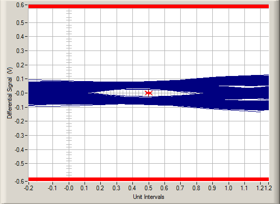
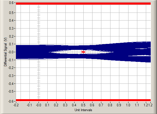
To demonstrate the reach extension capability of the DS160PR1601, two comparative setups are constructed. In first setup as shown in #X3590 there is no redriver in the PCIe 5.0 link. #FIG_L1S_HK3_BTB shows eye diagram at the end of the link using SigTest. In second setup as shown in #GUID-061CC0D4-53D5-4E4F-9D6B-47062873D590, the DS160PR1601 is inserted in the middle to extend link reach. #FIG_QSP_3K3_BTB shows SigTest eye diagram.
 Figure 8-4 PCIe 4.0 link Baseline
Setup Without Redriver – Eye Diagram Using SigTest
 Figure 8-6 PCIe 4.0 Link Setup with
the DS160PR1601 – Eye Diagram Using SigTest
Figure 8-6 PCIe 4.0 Link Setup with
the DS160PR1601 – Eye Diagram Using SigTestTable 8-1 summarizes the PCIe 4.0 links without and with the DS160PR1601. The illustration shows that redriver is capable of ≅16 dB (additional) reach extension at PCIe 4.0 speed with EQ = 15 and flat_gain = 101. Note: actual reach extension depends on various signal integrity factors. It is recommended to run signal intergrity simulations with all the components in the link to get any guidance.
| Setup | Pre Channel Loss | Post Channel Loss | Total Loss | Eye at BER 1E-12 | SigTest Pass? |
|---|---|---|---|---|---|
| Baseline – no DUT | — | — | ≅27 dB | 29 ps, 48 mV | Pass |
| With DUT (DS160PR1601) | ≅25 dB | ≅18 dB | ≅43 dB | 30 ps, 55 mV | Pass |