SNLS590C August 2018 – June 2021 DS250DF230
PRODUCTION DATA
- 1 Features
- 2 Applications
- 3 Description
- 4 Revision History
- 5 Description (continued)
- 6 Pin Configuration and Functions
- 7 Specifications
-
8 Detailed Description
- 8.1 Overview
- 8.2 Functional Block Diagram
- 8.3
Feature Description
- 8.3.1 Device Data Path Operation
- 8.3.2 Signal Detect
- 8.3.3 Continuous Time Linear Equalizer (CTLE)
- 8.3.4 Variable Gain Amplifier (VGA)
- 8.3.5 Cross-Point Switch
- 8.3.6 Decision Feedback Equalizer (DFE)
- 8.3.7 Clock and Data Recovery (CDR)
- 8.3.8 Calibration Clock
- 8.3.9 Differential Driver With FIR Filter
- 8.3.10 Debug Features
- 8.3.11 Interrupt Signals
- 8.4 Device Functional Modes
- 8.5 Programming
- 8.6 Register Maps
- 9 Application and Implementation
- 10Power Supply Recommendations
- 11Layout
- 12Device and Documentation Support
- 13Electrostatic Discharge Caution
- 14Glossary
- 15Mechanical, Packaging, and Orderable Information
Package Options
Mechanical Data (Package|Pins)
Thermal pad, mechanical data (Package|Pins)
- RTV|32
Orderable Information
3 Description
The DS250DF230 is a dual-channel multi-rate retimer with integrated signal conditioning. The device is used to extend the reach and robustness of long, lossy, crosstalk-impaired high-speed serial links and while achieving a bit error rate (BER) of 10–15 or less.
Each channel of the DS250DF230 independently locks to serial data rates in a continuous range from 19.6 Gbps to 25.8 Gbps or to any supported sub-rate (÷2 and ÷4), including key data rates such as 12.16512 Gbps, 9.8304 Gbps, and 6.144 Gbps.
The DS250DF230 is offered in two package options, 36-pin NFBGA and 32-pin QFN, with compact body sizes of 5 × 5 mm. The NFBGA (ZLS) package offers robust performance and ease of design with minimal BOM footprint, while the QFN (RTV) package offers similar performance characteristics with improved thermal performance supporting PCB temperatures up to 105°C without the need for a heat sink.
| PART NUMBER | PACKAGE | BODY SIZE (NOM) |
|---|---|---|
| DS250DF230ZLS | NFBGA (36) | 5.00 mm × 5.00 mm |
| DS250DF230RTV | QFN (32) | 5.00 mm × 5.00 mm |
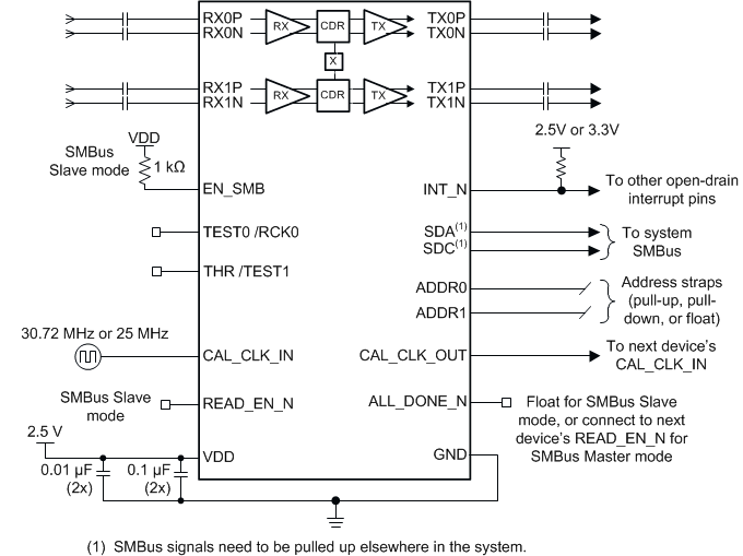
 Simplified Schematic