SNLS590C August 2018 – June 2021 DS250DF230
PRODUCTION DATA
- 1 Features
- 2 Applications
- 3 Description
- 4 Revision History
- 5 Description (continued)
- 6 Pin Configuration and Functions
- 7 Specifications
-
8 Detailed Description
- 8.1 Overview
- 8.2 Functional Block Diagram
- 8.3
Feature Description
- 8.3.1 Device Data Path Operation
- 8.3.2 Signal Detect
- 8.3.3 Continuous Time Linear Equalizer (CTLE)
- 8.3.4 Variable Gain Amplifier (VGA)
- 8.3.5 Cross-Point Switch
- 8.3.6 Decision Feedback Equalizer (DFE)
- 8.3.7 Clock and Data Recovery (CDR)
- 8.3.8 Calibration Clock
- 8.3.9 Differential Driver With FIR Filter
- 8.3.10 Debug Features
- 8.3.11 Interrupt Signals
- 8.4 Device Functional Modes
- 8.5 Programming
- 8.6 Register Maps
- 9 Application and Implementation
- 10Power Supply Recommendations
- 11Layout
- 12Device and Documentation Support
- 13Electrostatic Discharge Caution
- 14Glossary
- 15Mechanical, Packaging, and Orderable Information
Package Options
Mechanical Data (Package|Pins)
Thermal pad, mechanical data (Package|Pins)
- RTV|32
Orderable Information
9.2.2 Active Cable Applications
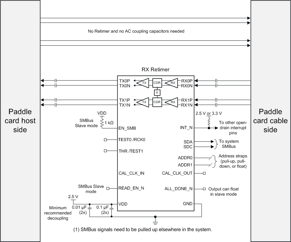
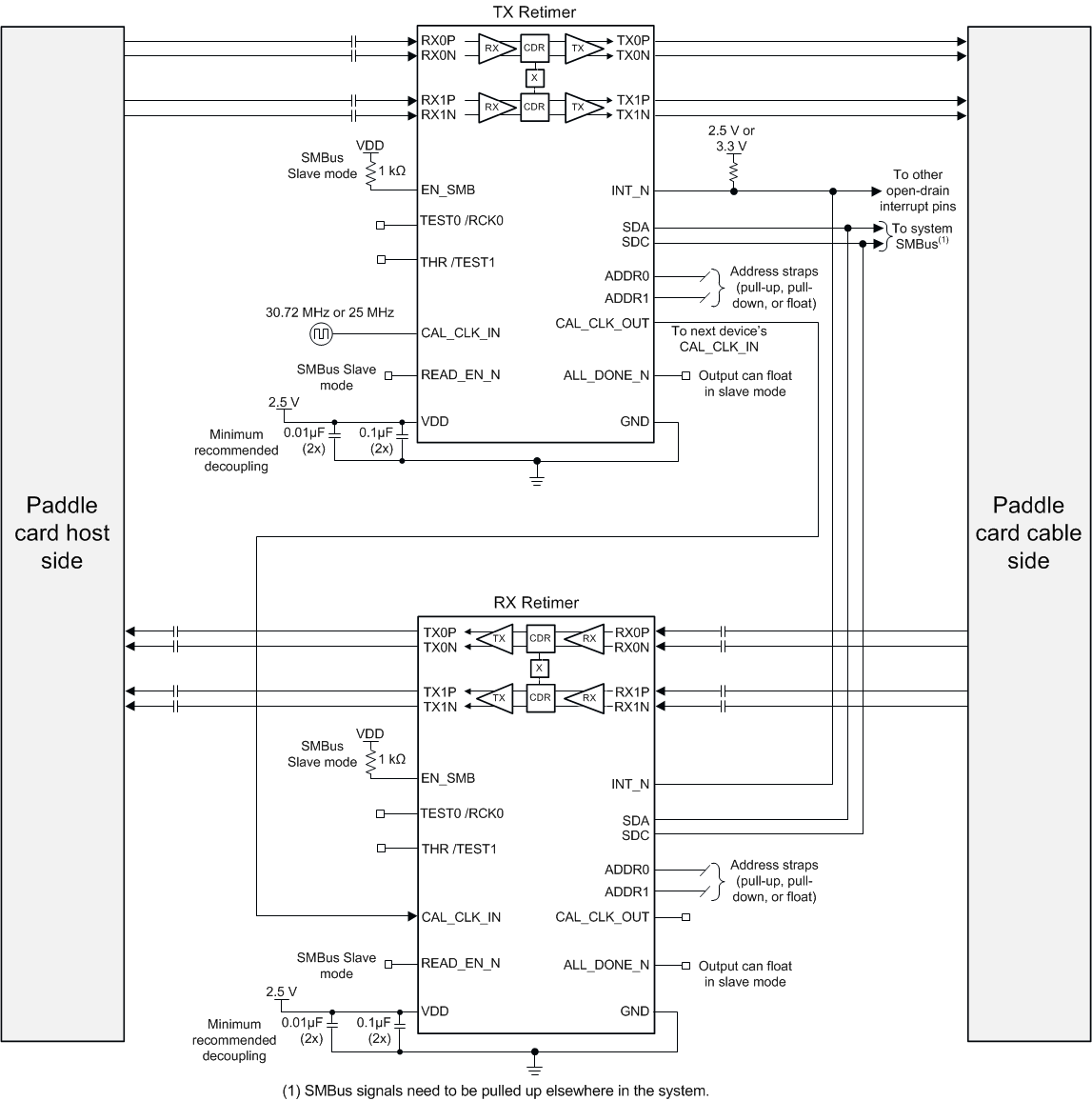
The DS250DF230 has strong equalization capabilities that allow it to recover data over long and/or thin-gauge copper cables. Two pcs DS250DF230s can be used on a QSFP28 paddle card to create a half-active cable assembly which is longer and/or thinner than passive cables. Alternatively, four pcs DS250DF230 devices can be used on a QSFP28 paddle card to create a full-active cable assembly and achieve even longer reach and/or thinner cables.
Figure 9-7 shows these configurations, Figure 9-8 shows an example simplified schematic for a half-active cable application, and Figure 9-9 shows an example simplified schematic for a full-active cable application.
 Figure 9-7 Active Cable
Application Block Diagram
 Figure 9-8 Half-Active Cable Application Schematic
 Figure 9-9 Full-Active Cable Application Schematic