SNLS544B September   2016  – October 2019 DS280BR820

PRODUCTION DATA.  

  1. Features
  2. Applications
  3. Description
    1.     Simplified Schematic
  4. Revision History
  5. Pin Configuration and Functions
    1.     Pin Functions
  6. Specifications
    1. 6.1 Absolute Maximum Ratings
    2. 6.2 ESD Ratings
    3. 6.3 Recommended Operating Conditions
    4. 6.4 Thermal Information
    5. 6.5 Electrical Characteristics
    6. 6.6 Electrical Characteristics – Serial Management Bus Interface
    7. 6.7 Timing Requirements – Serial Management Bus Interface
    8. 6.8 Typical Characteristics
  7. Detailed Description
    1. 7.1 Overview
    2. 7.2 Functional Block Diagram
    3. 7.3 Feature Description
      1. 7.3.1 Device Data Path Operation
      2. 7.3.2 AC-Coupled Receiver Inputs
      3. 7.3.3 Signal Detect
      4. 7.3.4 2-Stage CTLE
      5. 7.3.5 Driver DC Gain Control
      6. 7.3.6 FIR Filter (Limiting Mode)
      7. 7.3.7 Configurable SMBus Address
    4. 7.4 Device Functional Modes
      1. 7.4.1 SMBus Slave Mode Configuration
      2. 7.4.2 SMBus Master Mode Configuration (EEPROM Self Load)
    5. 7.5 Programming
      1. 7.5.1 Transfer of Data with the SMBus Interface
    6. 7.6 Register Maps
      1. 7.6.1 Register Types: Global, Shared, and Channel
      2. 7.6.2 Global Registers: Channel Selection and ID Information
        1. Table 2. Global Register Map
      3. 7.6.3 Shared Registers
        1. Table 3. Shared Register Map
      4. 7.6.4 Channel Registers
        1. Table 4. Channel Register Map
  8. Application and Implementation
    1. 8.1 Application Information
    2. 8.2 Typical Applications
      1. 8.2.1 Backplane and Mid-Plane Reach Extension
        1. 8.2.1.1 Design Requirements
        2. 8.2.1.2 Detailed Design Procedure
      2. 8.2.2 Front-Port Applications
        1. 8.2.2.1 Design Requirements
        2. 8.2.2.2 Detailed Design Procedure
      3. 8.2.3 Application Curves
        1. 8.2.3.1 Pattern Generator Characteristics
        2. 8.2.3.2 Equalizing Moderate Pre-Channel Loss
        3. 8.2.3.3 Equalizing High Pre-Channel Loss
        4. 8.2.3.4 Equalizing High Pre-Channel Loss and Moderate Post-Channel Loss
        5. 8.2.3.5 Output in FIR Limiting Mode with 16T Pattern
    3. 8.3 Initialization Set Up
  9. Power Supply Recommendations
  10. 10Layout
    1. 10.1 Layout Guidelines
    2. 10.2 Layout Examples
      1. 10.2.1 Stripline Example
      2. 10.2.2 Microstrip Example
  11. 11Device and Documentation Support
    1. 11.1 Documentation Support
      1. 11.1.1 Related Documentation
    2. 11.2 Receiving Notification of Documentation Updates
    3. 11.3 Trademarks
    4. 11.4 Electrostatic Discharge Caution
    5. 11.5 Glossary

Package Options

Mechanical Data (Package|Pins)
Thermal pad, mechanical data (Package|Pins)
Orderable Information

Typical Applications

The DS280BR820 is typically used in three main application scenarios:

  1. Backplane and mid-plane reach extension
  2. Front-port eye opening for copper and optical applications
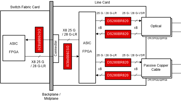
DS280BR820 application_block_diagram.gifFigure 6. Typical Application Diagram

NOTE

TI recommends to AC couple the DS280BR820's high-speed outputs. In some cases, ASIC or FPGA SerDes receivers support DC coupling, and it may be desirable to DC couple the DS280BR820 output with the ASIC/FPGA RX input to reduce the PCB area which would normally be consumed by AC coupling capacitors. To DC couple the DS280BR820 output with an ASIC RX input, the ASIC RX must support DC coupling and it must support an input common mode voltage of 1.05 V. To determine if the ASIC RX supports DC coupling, here are some items to consider based on Figure 7:

  1. The ASIC RX must be AC coupled on-chip.
  2. The ASIC RX should not force a DC bias on the RX pins.
  3. System designers should ensure that when the PCB powers on, the power supply rails are appropriately sequenced to prevent the DS280BR820's output common mode voltage from forward-biasing the ESD structure of the ASIC or violating the absolute maximum input voltage specifications of the ASIC.
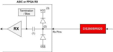
DS280BR820 DC_coupling_requirements.gifFigure 7. Considerations for DC Coupling to ASIC RX