SNLS538B September 2016 – February 2024 DS280DF810
PRODUCTION DATA
- 1
- 1 Features
- 2 Applications
- 3 Description
- 4 Pin Configuration and Functions
-
5 Specifications
- 5.1 Absolute Maximum Ratings
- 5.2 ESD Ratings
- 5.3 Recommended Operating Conditions
- 5.4 Thermal Information
- 5.5 Electrical Characteristics
- 5.6 Timing Requirements, Retimer Jitter Specifications
- 5.7 Timing Requirements, Retimer Specifications
- 5.8 Timing Requirements, Recommended Calibration Clock Specifications
- 5.9 Recommended SMBus Switching Characteristics (Target Mode)
- 5.10 Recommended SMBus Switching Characteristics (Controller Mode)
- 5.11 Typical Characteristics
-
6 Detailed Description
- 6.1 Overview
- 6.2 Functional Block Diagram
- 6.3
Feature Description
- 6.3.1
Device Data Path Operation
- 6.3.1.1 AC-Coupled Receiver and Transmitter
- 6.3.1.2 Signal Detect
- 6.3.1.3 Continuous Time Linear Equalizer (CTLE)
- 6.3.1.4 Variable Gain Amplifier (VGA)
- 6.3.1.5 2x2 Cross-Point Switch
- 6.3.1.6 Decision Feedback Equalizer (DFE)
- 6.3.1.7 Clock and Data Recovery (CDR)
- 6.3.1.8 Calibration Clock
- 6.3.1.9 Differential Driver with FIR Filter
- 6.3.2 Debug Features
- 6.3.1
Device Data Path Operation
- 6.4 Device Functional Modes
- 6.5 Programming
- 6.6 Register Maps
- 7 Application and Implementation
- 8 Device and Documentation Support
- 9 Revision History
- 10Mechanical, Packaging, and Orderable Information
Package Options
Refer to the PDF data sheet for device specific package drawings
Mechanical Data (Package|Pins)
- ABW|135
- ABV|135
Thermal pad, mechanical data (Package|Pins)
Orderable Information
7.4.2 Layout Example
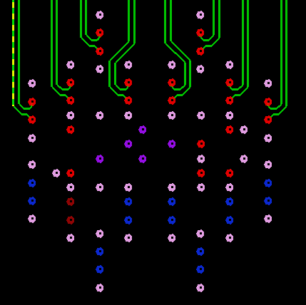
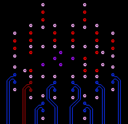
The following example layout demonstrates how all signals can be escaped from the BGA array using stripline routing on a generic 28-layer stackup. This example layout assumes the following:
- Trace width: 0.127mm (5 mil)
- Trace edge-to-edge spacing: 0.152mm (6 mil)
- VIA finished hole size (diameter): 0.203mm (8 mil)
- VIA drilled hole size: 0.254mm (10 mil)
- VIA-to-VIA spacing: 1.0mm (39 mil), to enhance PCB manufacturability
- No VIA-in-pad used
Note that many other escape routing options exist using different trace width and spacing combinations. The optimum trace width and spacing will depend on the PCB material, PCB routing density, and other factors.
 Figure 7-8 Top Layer
 Figure 7-10 Internal Signal Layer 2
 Figure 7-9 Internal Signal Layer 1
 Figure 7-11 Bottom Layer