SNLS542C October 2016 – December 2020 DS280MB810
PRODUCTION DATA
- 1 Features
- 2 Applications
- 3 Description
- 4 Revision History
- 5 Description (continued)
- 6 Pin Configuration and Functions
- 7 Specifications
- 8 Detailed Description
- 9 Application and Implementation
- 10Power Supply Recommendations
- 11Layout
- 12Device and Documentation Support
- 13Mechanical, Packaging, and Orderable Information
Package Options
Mechanical Data (Package|Pins)
- ZBL|135
Thermal pad, mechanical data (Package|Pins)
Orderable Information
9.2.3.3 Equalizing High Pre-Channel Loss
This example application result demonstrates the DS280MB810 equalizing for pre-channel insertion loss introduced by an FR4 channel.
 Figure 9-16 10 in input channel and minimal output channel test setup
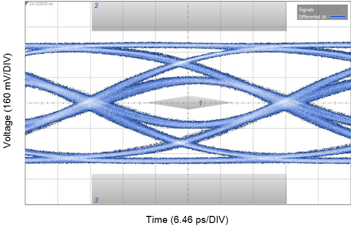
 Figure 9-17 25.78125 Gbps CAUI-4 Eye Mask with 10 in input channel and minimal output channel
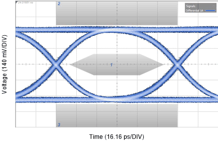
 Figure 9-18 10.3125 Gbps nPPI Eye Mask with 10 in input channel and minimal output channel
Table 9-3 Settings and Measurements for CAUI-4 and nPPI with 10 in input channel and minimal output channel
| 25.78125 Gbps (CAUI-4) | 10.3125 Gbps (nPPI) | |
|---|---|---|
| Transmission Line 1 | 10 in 5 mil FR4 + 8 in SMA cable | 10 in 5 mil FR4 + 8 in SMA cable |
| DS280MB810 Rx Channel Loss | 22 dB @ 12.9 GHz | 10 dB @ 5.2 GHz |
| DS280MB810 Tx Channel Loss | 4.5 dB @ 12.9 GHz | 2 dB @ 5.2 GHz |
| EQ BST1 | 6 | 6 |
| EQ BST2 | 1 | 1 |
| EQ BW | 3 | 3 |
| VOD | 3 | 2 |
| EQ DC Gain Mode | Low | Low |
| Total Jitter @ 1E-15 | 11.3 psP-P | 13.5 psP-P |
| Differential Eye Height @ 1E-15 | 210 mVP-P | 532 mVP-P |
| Mask violations | 0 | 0 |