SNLS683 june 2023 DS320PR1601
PRODUCTION DATA
- 1
- 1 Features
- 2 Applications
- 3 Description
- 4 Revision History
- 5 Pin Configuration and Functions
- 6 Specifications
- 7 Detailed Description
- 8 Programming
- 9 Application and Implementation
- 10Device and Documentation Support
- 11Mechanical, Packaging, and Orderable Information
Package Options
Mechanical Data (Package|Pins)
- ZDG|354
Thermal pad, mechanical data (Package|Pins)
Orderable Information
9.2.1.3 Application Curves
The DS320PR1601 is a linear redriver that can be used to extend channel reach of a PCIe link. Normally, PCIe-compliant Tx and Rx are equipped with signal-conditioning functions and can handle channel losses of up to 36 dB at 32 Gbps (16 GHz) PCIe 5.0. With the DS320PR1601, the total channel loss between a PCIe root complex and an end point can be extended up to 52 dB (18 dB additional) at 16 GHz.
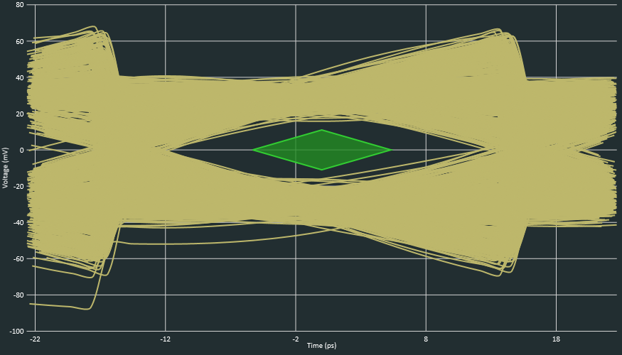
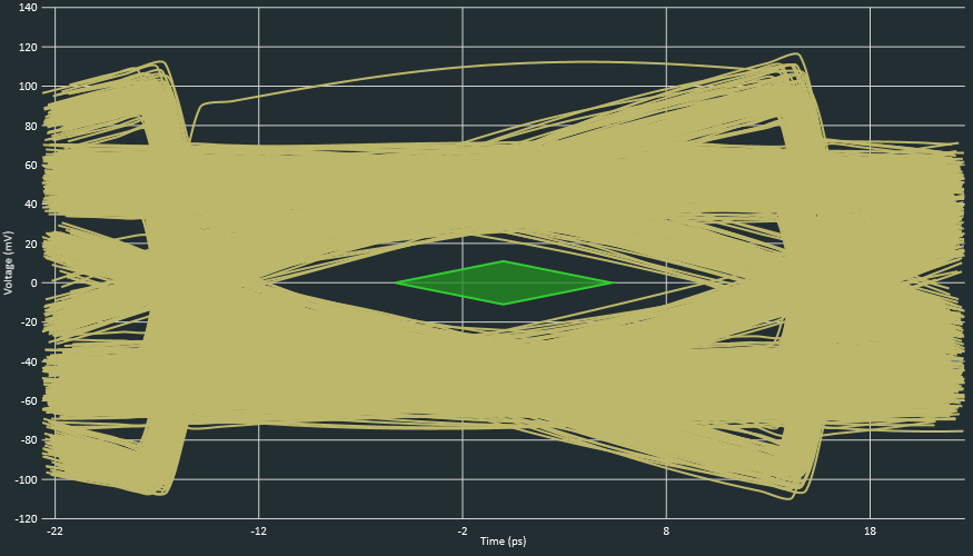
To demonstrate the reach extension capability of the DS320PR1601, two comparative setups are constructed. In first setup as shown in Figure 9-3 there is no redriver in the PCIe 5.0 link. Figure 9-4 shows eye diagram at the end of the link using SigTest. In second setup as shown in Figure 9-5, the DS320PR1601 is inserted in the middle to extend link reach. Figure 9-6 shows SigTest eye diagram.
 Figure 9-3 PCIe 5.0 Link
Baseline Setup Without Redriver – the Link Elements
 Figure 9-5 PCIe 5.0 Link Setup
with the DS320PR1601 – the Link Elements
 Figure 9-4 PCIe 5.0 link
Baseline Setup Without Redriver – Eye Diagram Using SigTest
 Figure 9-6 PCIe 5.0 Link Setup
with the DS320PR1601 – Eye Diagram Using SigTest
Figure 9-6 PCIe 5.0 Link Setup
with the DS320PR1601 – Eye Diagram Using SigTestTable 9-1 provides the PCIe 5.0 links without and with the DS320PR1601. The illustration shows that redriver is capable of ≅18 dB (additional) reach extension at PCIe 5.0 speed with EQ = 12 (15 dB) and flat_gain = 011 (-1.2 dB). Note: actual reach extension depends on various signal integrity factors. It is recommended to run signal integrity simulations with all the components in the link to get any guidance.
| Setup | Pre Channel Loss | Post Channel Loss | Total Loss | Eye at BER 1E-12 | SigTest Pass? |
|---|---|---|---|---|---|
| Baseline – no DUT | — | — | ≅36 dB | 13.0 ps, 27.8 mV | Pass |
| With DUT (DS320PR1601) | ≅27 dB | ≅25 dB | ≅52 dB | 13.5 ps, 31.2 mV | Pass |