SNLS374D May 1998 – January 2015 DS8921
PRODUCTION DATA.
- 1 Features
- 2 Applications
- 3 Description
- 4 Revision History
- 5 Pin Configuration and Functions
-
6 Specifications
- 6.1 Absolute Maximum Ratings
- 6.2 ESD Ratings
- 6.3 Recommended Operating Conditions
- 6.4 Electrical Characteristics
- 6.5 Receiver Switching Characteristics
- 6.6 Driver Switching Characteristics: Single-Ended Characteristics
- 6.7 Driver Switching Characteristics: Differential Characteristics
- 6.8 Typical Characteristics
- 7 Parameter Measurement Information
- 8 Detailed Description
- 9 Application and Implementation
- 10Power Supply Recommendations
- 11Layout
- 12Device and Documentation Support
- 13Mechanical, Packaging, and Orderable Information
Package Options
Mechanical Data (Package|Pins)
- D|8
Thermal pad, mechanical data (Package|Pins)
Orderable Information
9 Application and Implementation
NOTE
Information in the following applications sections is not part of the TI component specification, and TI does not warrant its accuracy or completeness. TI’s customers are responsible for determining suitability of components for their purposes. Customers should validate and test their design implementation to confirm system functionality.
9.1 Application Information
The DS8921 is a differential line driver and receiver pair in a single package, designed for applications for the ST506, ST412, and ESDI Disk Drive Standards. The DS8921 is compatible to EIA RS-422 signaling standards, supporting 200-mV input sensitivity across a ±7-V common mode operating range. This transceiver is intended for driving differential signal across long transmission lines and translating received differential signals into their CMOS/TTL single-ended equivalence. The DS8921 transmits and reproduces received data in communications links where ground reference difference, or noisy environment are common.
9.2 Typical Application
Figure 11 shows a typical implementation of the DS8921x device in a ST506 and ST412 disk drive application. The differential outputs of the driver are connected to a twisted-pair transmission line, carrying data from the driver to the differential receiver at the other end of the cable. A differential termination resistor should be connected across the input pins of the receiver.
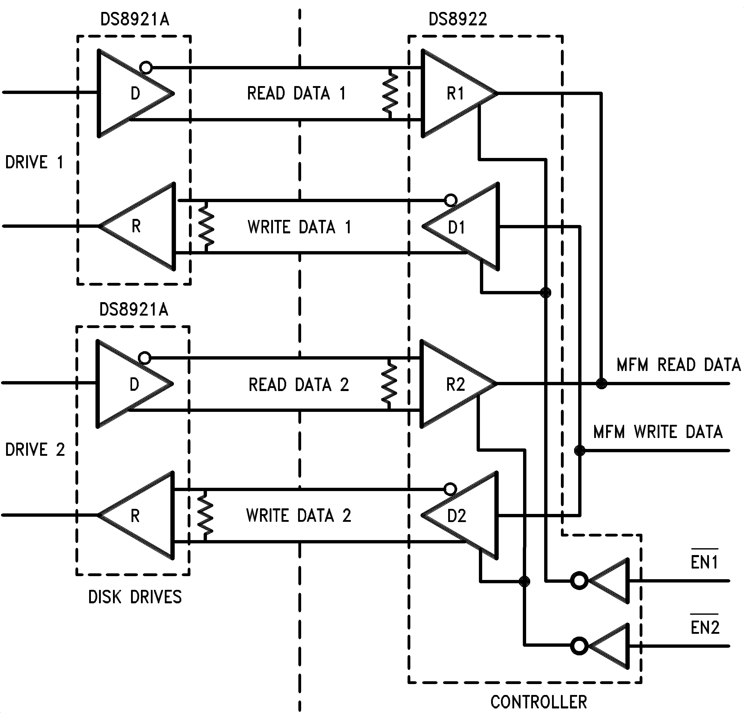 Figure 11. ST506 and ST412 Application
9.2.1 Design Requirements
- Apply TTL or LVCMOS signal to driver input at DI
- Transmit complementary outputs at DO+ and DO-
- Receive complimentary input signals at RI+ and RI-
- Receive TTL output signal at RO
- Use controlled-impedance transmission lines such as printed circuit board traces, twisted-pair wires or parallel wire cable
- Place terminating resistor at the far end of the differential pair
9.2.2 Detailed Design Procedure
- Connect VCC and GND pins to the power and ground planes of the printed circuit board, with 0.1-uF bypass capacitor
- Use TTL/LVCMOS logic levels at DI and RO
- Use controlled-impedance transmission media for the differential signals DI+- and RO+-
- Place a terminating resistor at the far-end of the differential pair to avoid reflection
- Ensure the received complimentary signals at RO+ and RO- are within the signal threshold of ±200 mV
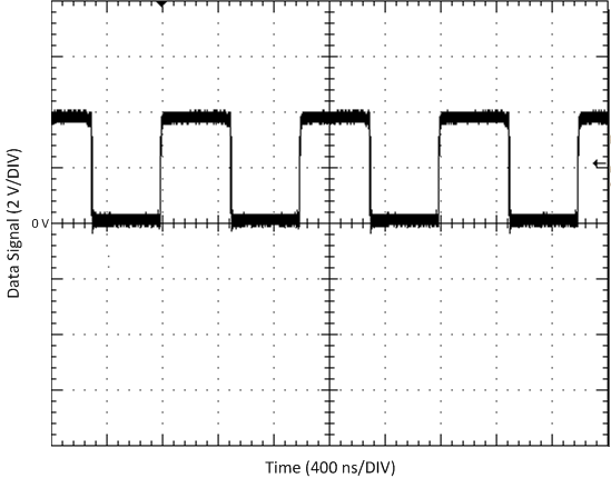
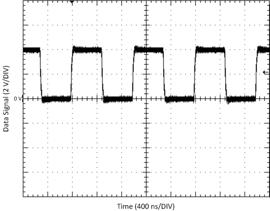
9.2.3 Application Curves
| 2.0 Mbps Single-Ended 1010 Data Pattern | ||
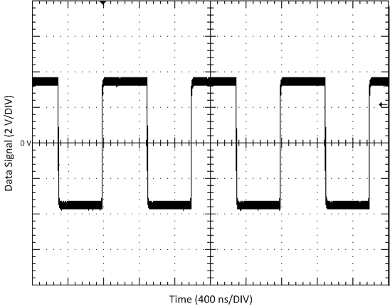
| 2.0 Mbps Differential Data Pattern | ||