SNLS374D May 1998 – January 2015 DS8921
PRODUCTION DATA.
- 1 Features
- 2 Applications
- 3 Description
- 4 Revision History
- 5 Pin Configuration and Functions
-
6 Specifications
- 6.1 Absolute Maximum Ratings
- 6.2 ESD Ratings
- 6.3 Recommended Operating Conditions
- 6.4 Electrical Characteristics
- 6.5 Receiver Switching Characteristics
- 6.6 Driver Switching Characteristics: Single-Ended Characteristics
- 6.7 Driver Switching Characteristics: Differential Characteristics
- 6.8 Typical Characteristics
- 7 Parameter Measurement Information
- 8 Detailed Description
- 9 Application and Implementation
- 10Power Supply Recommendations
- 11Layout
- 12Device and Documentation Support
- 13Mechanical, Packaging, and Orderable Information
Package Options
Mechanical Data (Package|Pins)
- D|8
Thermal pad, mechanical data (Package|Pins)
Orderable Information
8 Detailed Description
8.1 Overview
The DS8921x devices are each a differential line driver and receiver pair in a single package. The devices are designed specifically for ST506, ST412, and ESDI disk drive standards, as well as RS-422 interface applications. The DS8921 and DS8921A are rated at a commercial temperature range of 0°C to 70°C, whereas the DS8921AT is rated at an extended temperature range of -40°C to +85°C.
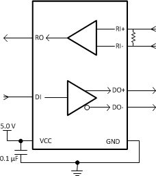
8.2 Functional Block Diagram
8.3 Feature Description
The DS8921x devices each contain a differential driver and receiver.
The driver converts a TTL or CMOS input to complementary outputs that provide differential drive to a twisted-pair or parallel wire transmission line. The receiver converts the differential signals at its input pins to a TTL output. The receiver offers an input sensitivity of ±200 mV and supports a common-mode input voltage of ±7 V.