SNLS209M November 2005 – January 2017 DS90C124 , DS90C241
PRODUCTION DATA.
- 1 Features
- 2 Applications
- 3 Description
- 4 Revision History
- 5 Pin Configuration and Functions
- 6 Specifications
- 7 Parameter Measurement Information
- 8 Detailed Description
- 9 Applications and Implementation
- 10Power Supply Recommendations
- 11Layout
- 12Device and Documentation Support
- 13Mechanical, Packaging, and Orderable Information
Package Options
Mechanical Data (Package|Pins)
- PFB|48
Thermal pad, mechanical data (Package|Pins)
Orderable Information
11 Layout
11.1 Layout Guidelines
Circuit board layout and stack-up for the LVDS SERDES devices must be designed to provide low-noise power feed to the device. Good layout practice also separates high frequency or high-level inputs and outputs to minimize unwanted stray noise pickup, feedback and interference. Power system performance may be greatly improved by using thin dielectrics (2 to 4 mils) for power and ground sandwiches. This arrangement provides plane capacitance for the PCB power system with low-inductance parasitics, which has proven especially effective at high frequencies, and makes the value and placement of external bypass capacitors less critical. External bypass capacitors must include both RF ceramic and tantalum electrolytic types. RF capacitors may use values in the range of 0.01 µF to 0.1 µF. Tantalum capacitors may be in the 2.2-µF to 10-µF range. Voltage rating of the tantalum capacitors must be at least 5 times the power supply voltage being used.
Surface mount capacitors are recommended due to their smaller parasitics. When using multiple capacitors per supply pin, place the smaller value closer to the pin. A large bulk capacitor is recommend at the point of power entry. This is typically in the 50-µF to 100-µF range and smooth low frequency switching noise. TI recommends connecting power and ground pins directly to the power and ground planes with bypass capacitors connected to the plane with via on both ends of the capacitor. Connecting power or ground pins to an external bypass capacitor increases the inductance of the path.
A small body size X7R chip capacitor, such as 0603, is recommended for external bypass. Its small body size reduces the parasitic inductance of the capacitor. The user must pay attention to the resonance frequency of these external bypass capacitors, usually in the range of 20 MHz to 30 MHz range. To provide effective bypassing, multiple capacitors are often used to achieve low impedance between the supply rails over the frequency of interest. At high frequency, it is also a common practice to use two vias from power and ground pins to the planes, reducing the impedance at high frequency.
Some devices provide separate power and ground pins for different portions of the circuit. This is done to isolate switching noise effects between different sections of the circuit. Separate planes on the PCB are typically not required. Pin Configuration and Functions typically provide guidance on which circuit blocks are connected to which power pin pairs. In some cases, an external filter many be used to provide clean power to sensitive circuits such as PLLs.
Use at least a four layer board with a power and ground plane. Place LVCMOS (LVTTL) signals away from the LVDS lines to prevent coupling from the LVCMOS lines to the LVDS lines. Closely-coupled differential lines of 100 Ω are typically recommended for LVDS interconnect. The closely coupled lines help to ensure that coupled noise appears as common-mode and thus is rejected by the receivers. The tightly coupled lines also radiate less.
Termination of the LVDS interconnect is required. For point-to-point applications, termination must be placed at both ends of the devices. Nominal value is 100 Ω to match the line’s differential impedance. Place the resistor as close to the transmitter DOUT± outputs and receiver RIN± inputs as possible to minimize the resulting stub between the termination resistor and device.
11.1.1 LVDS Interconnect Guidelines
See AN-1108 Channel-Link PCB and Interconnect Design-In Guidelines (SNLA008) and AN-905 Transmission Line RAPIDESIGNER© Operation and Applications Guide (SNLA035) for full details.
- Use 100-Ω coupled differential pairs
- Use the S/2S/3S rule in spacings
- S = space between the pair
- 2S = space between pairs
- 3S = space to LVCMOS/LVTTL signal
- Minimize the number of vias
- Use differential connectors when operating above 500-Mbps line speed
- Maintain balance of the traces
- Minimize skew within the pair
- Terminate as close to the TX outputs and RX inputs as possible
Additional general guidance can be found in the LVDS Owner’s Manual available in PDF format from the TI web site at: www.ti.com/lvds.
11.2 Layout Example
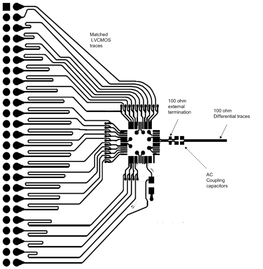
Figure 31 shows the input LVCMOS traces and output high-speed, 100-Ω differential traces from the DS90C241 EVM.
 Figure 31. DS90C241 Layout Example from DS90C241 EVM
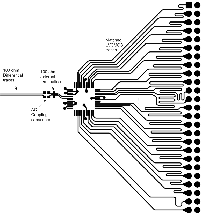
Figure 32 shows the input high-speed, 100-Ω differential traces and the output LVCMOS traces and from the DS90C124 EVM.
 Figure 32. DS90C124 Layout Example from DS90C124 EVM
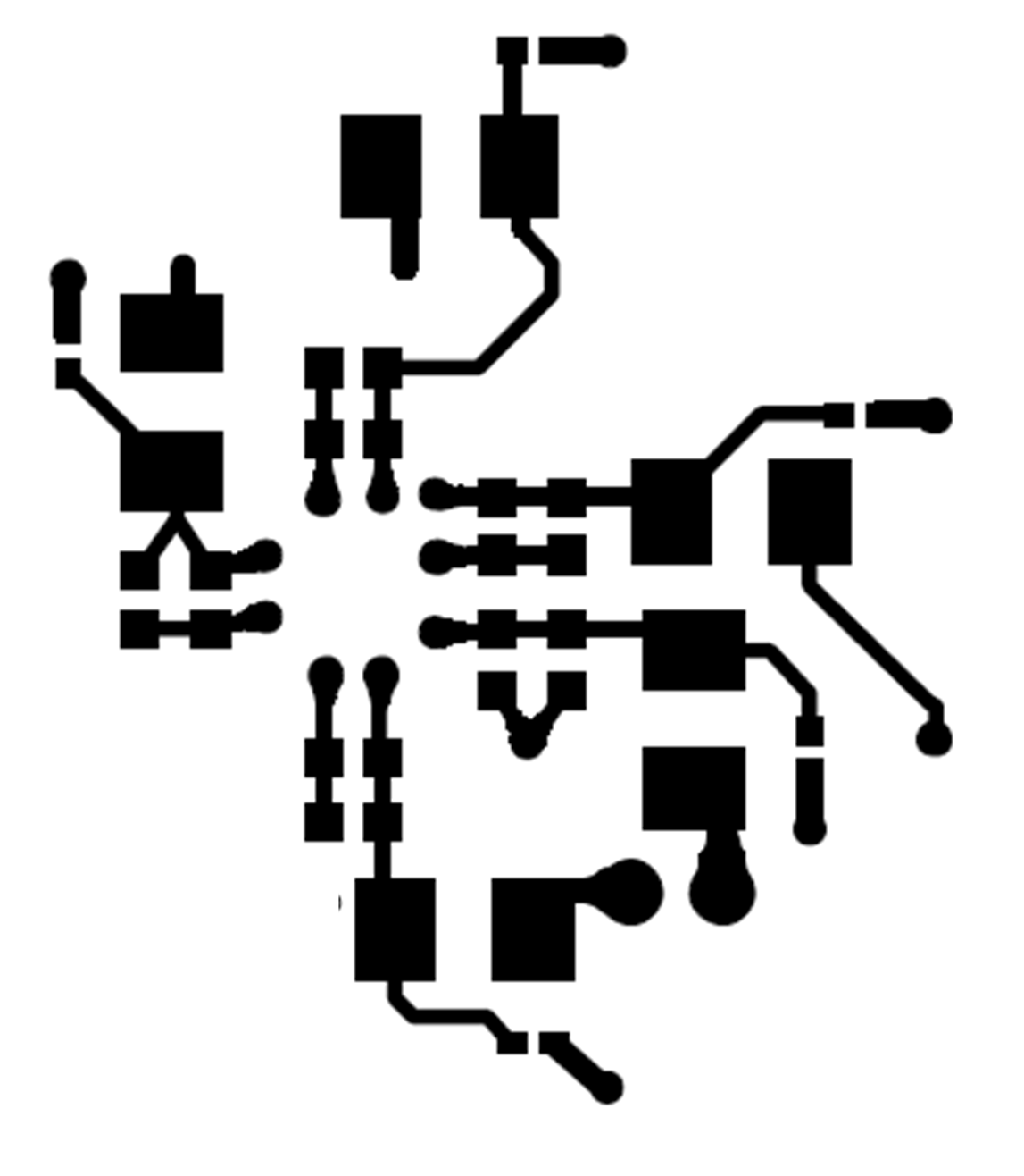
Figure 33 shows the power decoupling from the DS90C241 EVM.
 Figure 33. DS90C241 Example Layout of Power Decoupling from EVM
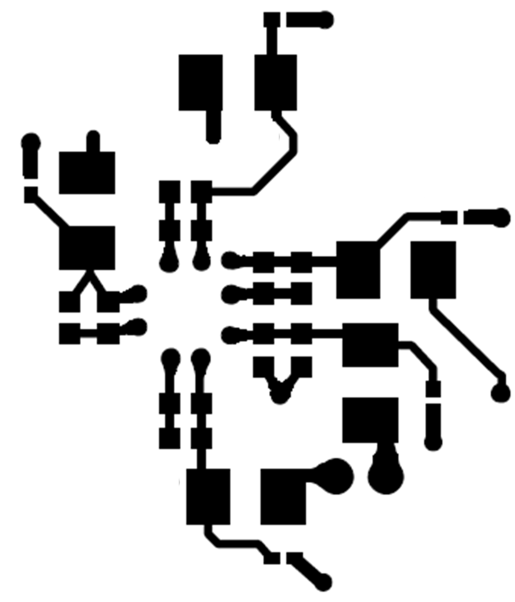
Figure 34 shows the power decoupling from the DS90C124 EVM.
 Figure 34. DS90C124 Example Layout of Power Decoupling from EVM