SNLS198C September 2005 – July 2021 DS90LV011AH
PRODUCTION DATA
- 1 Features
- 2 Applications
- 3 Description
- 4 Revision History
- 5 Pin Configuration and Functions
- 6 Specifications
- 7 Parameter Measurement Information
- 8 Detailed Description
- 9 Application and Implementation
- 10Power Supply Recommendations
- 11Layout
- 12Device and Documentation Support
- 13Mechanical, Packaging, and Orderable Information
Package Options
Mechanical Data (Package|Pins)
- DBV|5
Thermal pad, mechanical data (Package|Pins)
Orderable Information
11.1.6 Decoupling
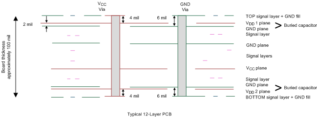
Each power or ground lead of a high-speed device should be connected to the PCB through a low inductance path. For best results, one or more vias are used to connect a power or ground pin to the nearby plane. TI recommends placing a via immediately adjacent to the pin to avoid adding trace inductance. Placing a power plane closer to the top of the board reduces the effective via length and its associated inductance.
 Figure 11-6 Low Inductance, High-Capacitance Power Connection
Bypass capacitors should be placed close to VDD pins. They can be placed conveniently near the corners or underneath the package to minimize the loop area. This extends the useful frequency range of the added capacitance. Small-physical-size capacitors, such as 0402 or even 0201, or X7R surface-mount capacitors should be used to minimize body inductance of capacitors. Each bypass capacitor is connected to the power and ground plane through vias tangent to the pads of the capacitor as shown in Figure 11-7(a).
An X7R surface-mount capacitor of size 0402 has about 0.5 nH of body inductance. At frequencies above 30 MHz or so, X7R capacitors behave as low-impedance inductors. To extend the operating frequency range to a few hundred MHz, an array of different capacitor values like 100 pF, 1 nF, 0.03 μF, and 0.1 μF are commonly used in parallel. The most effective bypass capacitor can be built using sandwiched layers of power and ground at a separation of 2 to 3 mils. With a 2-mil FR4 dielectric, there is approximately 500 pF per square inch of PCB. Refer back to Figure 8 for some examples. Many high-speed devices provide a low-inductance GND connection on the backside of the package. This center dap must be connected to a ground plane through an array of vias. The via array reduces the effective inductance to ground and enhances the thermal performance of the small Surface Mount Technology (SMT) package. Placing vias around the perimeter of the dap connection ensures proper heat spreading and the lowest possible die temperature. Placing high-performance devices on opposing sides of the PCB using two GND planes (as shown in Figure 9-3) creates multiple paths for heat transfer. Often thermal PCB issues are the result of one device adding heat to another, resulting in a very high local temperature.
Multiple paths for heat transfer minimize this possibility. In many cases the GND dap that is so important for heat dissipation makes the optimal decoupling layout impossible to achieve due to insufficient pad-to-dap spacing as shown in Figure 11-7(b). When this occurs, placing the decoupling capacitor on the backside of the board keeps the extra inductance to a minimum. It is important to place the VDD via as close to the device pin as possible while still allowing for sufficient solder mask coverage. If the via is left open, solder may flow from the pad and into the via barrel. This will result in a poor solder connection.
 Figure 11-7 Typical Decoupling Capacitor Layouts
At least two or three times the width of an individual trace should separate single-ended traces and differential pairs to minimize the potential for crosstalk. Single-ended traces that run in parallel for less than the wavelength of the rise or fall times usually have negligible crosstalk. Increase the spacing between signal paths for long parallel runs to reduce crosstalk. Boards with limited real estate can benefit from the staggered trace layout, as shown in Figure 11-8.
 Figure 11-8 Staggered
Trace Layout
Figure 11-8 Staggered
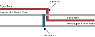
Trace LayoutThis configuration lays out alternating signal traces on different layers. Thus, the horizontal separation between traces can be less than 2 or 3 times the width of individual traces. To ensure continuity in the ground signal path, TI recommends having an adjacent ground via for every signal via, as shown in Figure 11-9. Note that vias create additional capacitance. For example, a typical via has a lumped capacitance effect of 1/2 pF to 1 pF in FR4.
 Figure 11-9 Ground
Via Location (Side View)
Figure 11-9 Ground
Via Location (Side View)Short and low-impedance connection of the device ground pins to the PCB ground plane reduces ground bounce. Holes and cutouts in the ground planes can adversely affect current return paths if they create discontinuities that increase returning current loop areas.
To minimize EMI problems, TI recommends avoiding discontinuities below a trace (for example, holes, slits, and so on) and keeping traces as short as possible. Zoning the board wisely by placing all similar functions in the same area, as opposed to mixing them together, helps reduce susceptibility issues.