SNLS044D May 2000 – July 2016 DS90LV047A
PRODUCTION DATA.
- 1 Features
- 2 Applications
- 3 Description
- 4 Revision History
- 5 Pin Configuration and Functions
- 6 Specifications
- 7 Parameter Measurement Information
- 8 Detailed Description
- 9 Application and Implementation
- 10Power Supply Recommendations
- 11Layout
- 12Device and Documentation Support
- 13Mechanical, Packaging, and Orderable Information
Package Options
Mechanical Data (Package|Pins)
Thermal pad, mechanical data (Package|Pins)
Orderable Information
8 Detailed Description
8.1 Overview
LVDS drivers and receivers are intended to be primarily used in an uncomplicated point-to-point configuration as is shown in Figure 23. This configuration provides a clean signaling environment for the fast edge rates of the drivers. The receiver is connected to the driver through a balanced media which may be a standard twisted pair cable, a parallel pair cable, or simply PCB traces. Typically, the characteristic differential impedance of the media is in the range of 100 Ω. A termination resistor of 100 Ω (selected to match the media), and is located as close to the receiver input pins as possible. The termination resistor converts the driver output current (current mode) into a voltage that is detected by the receiver. Other configurations are possible such as a multi-receiver configuration, but the effects of a mid-stream connector(s), cable stub(s), and other impedance discontinuities as well as ground shifting, noise margin limits, and total termination loading must be taken into account.
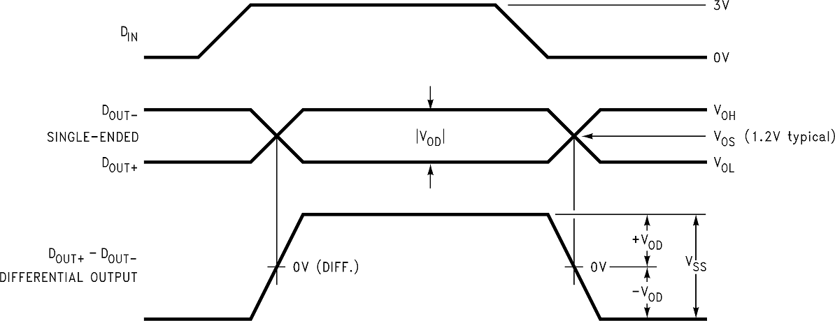
The DS90LV047A differential line driver is a balanced current source design. A current mode driver, generally speaking has a high output impedance and supplies a constant current for a range of loads (a voltage mode driver on the other hand supplies a constant voltage for a range of loads). Current is switched through the load in one direction to produce a logic state and in the other direction to produce the other logic state. The output current is typically 3.1 mA, a minimum of 2.5 mA, and a maximum of 4.5 mA. The current mode driver requires (as discussed above) that a resistive termination be employed to terminate the signal and to complete the loop as shown in Figure 23. AC or unterminated configurations are not allowed. The 3.1-mA loop current develops a differential voltage of 310 mV across the 100-Ω termination resistor which the receiver detects with a 250-mV minimum differential noise margin, (driven signal minus receiver threshold (250 mV – 100 mV = 150 mV). The signal is centered around +1.2 V (Driver Offset, VOS) with respect to ground as shown in Figure 22.
NOTE
The steady-state voltage (VSS) peak-to-peak swing is twice the differential voltage (VOD) and is typically 620 mV.
The current mode driver provides substantial benefits over voltage mode drivers, such as an RS-422 driver. Its quiescent current remains relatively flat versus switching frequency. Whereas the RS-422 voltage mode driver increases exponentially in most case from 20 MHz to 50 MHz. This is due to the overlap current that flows between the rails of the device when the internal gates switch. Whereas the current mode driver switches a fixed current between its output without any substantial overlap current. This is similar to some ECL and PECL devices, but without the heavy static ICC requirements of the ECL/PECL designs. LVDS requires > 80% less current than similar PECL devices. AC specifications for the driver are a tenfold improvement over other existing RS-422 drivers.
The TRI-STATE function allows the driver outputs to be disabled, thus obtaining an even lower power state when the transmission of data is not required.
8.2 Functional Block Diagram

8.3 Feature Description
8.3.1 LVDS Fail-Safe
This section addresses the common concern of fail-safe biasing of LVDS interconnects, specifically looking at the DS90LV047A driver outputs and the DS90LV048A receiver inputs.
The LVDS receiver is a high-gain, high-speed device that amplifies a small differential signal (20 mV) to CMOS logic levels. Due to the high gain and tight threshold of the receiver, take care to prevent noise from appearing as a valid signal.
The internal fail-safe circuitry of the receiver is designed to source or sink a small amount of current, providing fail-safe protection (a stable known state of HIGH output voltage) for floating, terminated, or shorted receiver inputs.
- Open Input Pins. The DS90LV048A is a quad receiver device, and if an application requires only 1, 2, or 3 receivers, the unused channel(s) inputs must be left OPEN. Do not tie unused receiver inputs to ground or any other voltages. The input is biased by internal high value pullup and pulldown resistors to set the output to a HIGH state. This internal circuitry ensures a HIGH, stable output state for open inputs.
- Terminated Input. If the DS90LV047A driver is disconnected (cable unplugged), or if the DS90LV047A driver is in a TRI-STATE or power-off condition, the receiver output is again in a HIGH state, even with the end of cable 100-Ω termination resistor across the input pins. The unplugged cable can become a floating antenna which can pick up noise. If the cable picks up more than 10 mV of differential noise, the receiver may see the noise as a valid signal and switch. To insure that any noise is seen as common-mode and not differential, a balanced interconnect must be used. Twisted pair cable offers better balance than flat ribbon cable.
- Shorted Inputs. If a fault condition occurs that shorts the receiver inputs together, thus resulting in a 0-V differential input voltage, the receiver output remains in a HIGH state. Shorted input fail-safe is not supported across the common-mode range of the device (GND to 2.4 V). It is only supported with inputs shorted and no external common-mode voltage applied.
External lower value pullup and pulldown resistors (for a stronger bias) may be used to boost fail-safe in the presence of higher noise levels. The pullup and pulldown resistors should be in the 5-kΩ to 15-kΩ range to minimize loading and waveform distortion to the driver. The common-mode bias point should be set to approximately 1.2 V (less than 1.75 V) to be compatible with the internal circuitry.
 Figure 22. Driver Output Levels
8.4 Device Functional Modes
Table 1 lists the functional modes DS90LV047A.
Table 1. Truth Table
| ENABLES | INPUT | OUTPUTS | ||
|---|---|---|---|---|
| EN | EN* | DIN | DOUT+ | DOUT− |
| H | L or Open | L | L | H |
| H | H | L | ||
| All other combinations of ENABLE inputs | X | Z | Z | |