SNLS045C July 1999 – July 2016 DS90LV048A
PRODUCTION DATA.
- 1 Features
- 2 Applications
- 3 Description
- 4 Revision History
- 5 Pin Configuration and Functions
- 6 Specifications
- 7 Parameter Measurement Information
- 8 Detailed Description
- 9 Application and Implementation
- 10Power Supply Recommendations
- 11Layout
- 12Device and Documentation Support
- 13Mechanical, Packaging, and Orderable Information
Package Options
Mechanical Data (Package|Pins)
Thermal pad, mechanical data (Package|Pins)
Orderable Information
8 Detailed Description
8.1 Overview
LVDS drivers and receivers are intended to be primarily used in an uncomplicated point-to-point configuration as shown in Figure 19. This configuration provides a clean signaling environment for the fast edge rates of the drivers. The receiver is connected to the driver through a balanced media which may be a standard twisted pair cable, a parallel pair cable, or simply PCB traces. Typically, the characteristic impedance of the media is in the range of 100 Ω. A termination resistor of 100 Ω (selected to match the media) is located as close to the receiver input pins as possible. The termination resistor converts the driver output (current mode) into a voltage that is detected by the receiver. Other configurations are possible such as a multi-receiver configuration, but the effects of a mid-stream connector(s), cable stub(s), and other impedance discontinuities as well as ground shifting, noise margin limits, and total termination loading must be considered.
The DS90LV048A differential line receiver is capable of detecting signals as low as 100 mV, over a ±1-V common-mode range centered around +1.2 V. This is related to the driver offset voltage which is typically +1.2 V. The driven signal is centered around this voltage and may shift ±1 V around this center point. The ±1-V shifting may be the result of a ground potential difference between the ground reference of the driver and the ground reference of the receiver, the common-mode effects of coupled noise, or a combination of the two. The AC parameters of both receiver input pins are optimized for a recommended operating input voltage range of 0 V to +2.4 V (measured from each pin to ground). The device operates for receiver input voltages up to VCC, but exceeding VCC turns on the ESD protection circuitry, which clamps the bus voltages.
The DS90LV048A has a flow-through pinout that allows for easy PCB layout. The LVDS signals on one side of the device easily allows for matching electrical lengths of the differential pair trace lines between the driver and the receiver as well as allowing the trace lines to be close together to couple noise as common-mode. Noise isolation is achieved with the LVDS signals on one side of the device and the TTL signals on the other side.
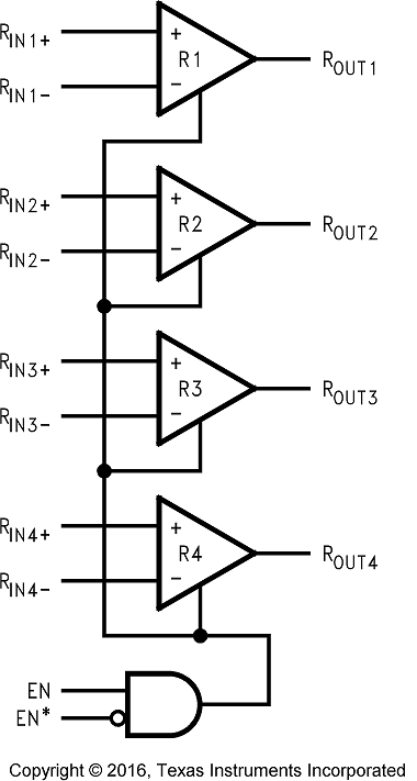
8.2 Functional Block Diagram

8.3 Feature Description
8.3.1 Fail-Safe Feature
The LVDS receiver is a high-gain, high-speed device that amplifies a small differential signal (20 mV) to CMOS logic levels. Due to the high gain and tight threshold of the receiver, take care to prevent noise from appearing as a valid signal.
The internal fail-safe circuitry of the receiver is designed to source or sink a small amount of current, providing fail-safe protection (a stable known state of HIGH output voltage) for floating, terminated or shorted receiver inputs.
- Open Input Pins. The DS90LV048A is a quad receiver device, and if an application requires only 1, 2, or 3 receivers, the unused channel(s) inputs must be left OPEN. Do not tie unused receiver inputs to ground or any other voltages. The input is biased by internal high value pullup and pulldown resistors to set the output to a HIGH state. This internal circuitry ensures a HIGH, stable output state for open inputs.
- Terminated Input. If the driver is disconnected (cable unplugged), or if the driver is in a TRI-STATE or power-off condition, the receiver output is again in a HIGH state, even with the end of cable 100-Ω termination resistor across the input pins. The unplugged cable can become a floating antenna which can pick up noise. If the cable picks up more than 10 mV of differential noise, the receiver may see the noise as a valid signal and switch. To ensure that any noise is seen as common-mode and not differential, a balanced interconnect should be used. Twisted pair cable offers better balance than flat ribbon cable.
- Shorted Inputs. If a fault condition occurs that shorts the receiver inputs together, thus resulting in a 0-V differential input voltage, the receiver output remains in a HIGH state. Shorted input fail-safe is not supported across the common-mode range of the device (GND to 2.4 V). It is only supported with inputs shorted and no external common-mode voltage applied.
External lower value pullup and pulldown resistors (for a stronger bias) may be used to boost fail-safe in the presence of higher noise levels. The pullup and pulldown resistors must be in the 5-kΩ to 15-kΩ range to minimize loading and waveform distortion to the driver. The common-mode bias point must be set to approximately 1.2 V (less than 1.75 V) to be compatible with the internal circuitry.
Additional information on fail-safe biasing of LVDS devices may be found in AN-1194 Failsafe Biasing of LVDS Interfaces (SNLA051).
8.4 Device Functional Modes
Table 1 lists the functional modes of the DS90LV048A.
Table 1. Truth Table
| ENABLES | INPUT | OUTPUT | |
|---|---|---|---|
| EN | EN* | RIN+ − RIN− | ROUT |
| H | L or Open | VID ≥ 0 V | H |
| VID ≤ −0.1 V | L | ||
| Full Fail-safe OPEN/SHORT or Terminated | H | ||
| All other combinations of ENABLE inputs | X | Z | |