SNLS499D April 2016 – October 2019 DS90UB914A-Q1
PRODUCTION DATA.
- 1 Features
- 2 Applications
- 3 Description
- 4 Revision History
- 5 Device Comparison Table
- 6 Pin Configuration and Functions
-
7 Specifications
- 7.1 Absolute Maximum Ratings
- 7.2 ESD Ratings
- 7.3 Recommended Operating Conditions
- 7.4 Thermal Information
- 7.5 Electrical Characteristics
- 7.6 AC Timing Specifications (SCL, SDA) - I2C-Compatible
- 7.7 Bidirectional Control Bus DC Timing Specifications (SCL, SDA) - I2C-Compatible
- 7.8 Deserializer Switching Characteristics
- 7.9 Typical Characteristics
- 8 Parameter Measurement Information
-
9 Detailed Description
- 9.1 Overview
- 9.2 Functional Block Diagram
- 9.3
Feature Description
- 9.3.1 Serial Frame Format
- 9.3.2 Line Rate Calculations for the DS90UB913A/914A
- 9.3.3 Deserializer Multiplexer Input
- 9.3.4 Error Detection
- 9.3.5 Synchronizing Multiple Cameras
- 9.3.6 General-Purpose I/O (GPIO) Descriptions
- 9.3.7 LVCMOS VDDIO Option
- 9.3.8 EMI Reduction
- 9.3.9 Pixel Clock Edge Select (TRFB / RRFB)
- 9.3.10 Power Down
- 9.4
Device Functional Modes
- 9.4.1 DS90UB913A/914A Operation With External Oscillator as Reference Clock
- 9.4.2 DS90UB913A/914A Operation With Pixel Clock From Imager as Reference Clock
- 9.4.3 MODE Pin on Deserializer
- 9.4.4 Clock-Data Recovery Status Flag (LOCK), Output Enable (OEN) and Output State Select (OSS_SEL)
- 9.4.5 Built-In Self Test
- 9.4.6 BIST Configuration and Status
- 9.4.7 Sample BIST Sequence
- 9.5 Programming
- 9.6 Register Maps
- 10Application and Implementation
- 11Power Supply Recommendations
- 12Layout
- 13Device and Documentation Support
- 14Mechanical, Packaging, and Orderable Information
Package Options
Mechanical Data (Package|Pins)
- RHS|48
Thermal pad, mechanical data (Package|Pins)
- RHS|48
Orderable Information
9.5.2 Description of Bidirectional Control Bus and I2C Modes
The I2C-compatible interface allows programming of the DS90UB913A-Q1, DS90UB914A-Q1, or an external remote device (such as image sensor) through the bidirectional control channel. Register programming transactions to/from the DS90UB913A-Q1/914A-Q1 chipset are employed through the clock (SCL) and data (SDA) lines. These two signals have open drain I/Os and both lines must be pulled-up to VDDIO by an external resistor. Pullup resistors or current sources are required on the SCL and SDA busses to pull them high when they are not being driven low. A logic LOW is transmitted by driving the output low. Logic HIGH is transmitted by releasing the output and allowing it to be pulled-up externally. The appropriate pullup resistor values will depend upon the total bus capacitance and operating speed. The DS90UB913A/914A I2C bus data rate supports up to 400 kbps according to I2C fast mode specifications.
For further description of general I2C communication, please refer to application note Understanding the I2C Bus (SLVA704). For more information on choosing appropriate pullup resistor values, please refer to application note I2C Bus Pullup Resistor Calculation (SLVA689).
 Figure 21. Write Byte
  Figure 22. Read Byte
  Figure 23. Basic Operation
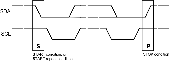
  Figure 24. Start and Stop Conditions