SNLS499D April 2016 – October 2019 DS90UB914A-Q1
PRODUCTION DATA.
- 1 Features
- 2 Applications
- 3 Description
- 4 Revision History
- 5 Device Comparison Table
- 6 Pin Configuration and Functions
-
7 Specifications
- 7.1 Absolute Maximum Ratings
- 7.2 ESD Ratings
- 7.3 Recommended Operating Conditions
- 7.4 Thermal Information
- 7.5 Electrical Characteristics
- 7.6 AC Timing Specifications (SCL, SDA) - I2C-Compatible
- 7.7 Bidirectional Control Bus DC Timing Specifications (SCL, SDA) - I2C-Compatible
- 7.8 Deserializer Switching Characteristics
- 7.9 Typical Characteristics
- 8 Parameter Measurement Information
-
9 Detailed Description
- 9.1 Overview
- 9.2 Functional Block Diagram
- 9.3
Feature Description
- 9.3.1 Serial Frame Format
- 9.3.2 Line Rate Calculations for the DS90UB913A/914A
- 9.3.3 Deserializer Multiplexer Input
- 9.3.4 Error Detection
- 9.3.5 Synchronizing Multiple Cameras
- 9.3.6 General-Purpose I/O (GPIO) Descriptions
- 9.3.7 LVCMOS VDDIO Option
- 9.3.8 EMI Reduction
- 9.3.9 Pixel Clock Edge Select (TRFB / RRFB)
- 9.3.10 Power Down
- 9.4
Device Functional Modes
- 9.4.1 DS90UB913A/914A Operation With External Oscillator as Reference Clock
- 9.4.2 DS90UB913A/914A Operation With Pixel Clock From Imager as Reference Clock
- 9.4.3 MODE Pin on Deserializer
- 9.4.4 Clock-Data Recovery Status Flag (LOCK), Output Enable (OEN) and Output State Select (OSS_SEL)
- 9.4.5 Built-In Self Test
- 9.4.6 BIST Configuration and Status
- 9.4.7 Sample BIST Sequence
- 9.5 Programming
- 9.6 Register Maps
- 10Application and Implementation
- 11Power Supply Recommendations
- 12Layout
- 13Device and Documentation Support
- 14Mechanical, Packaging, and Orderable Information
Package Options
Mechanical Data (Package|Pins)
- RHS|48
Thermal pad, mechanical data (Package|Pins)
- RHS|48
Orderable Information
9.4.3 MODE Pin on Deserializer
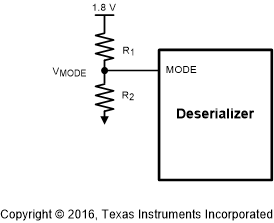
The MODE pin on the Deserializer can be used to configure the device to work in the 12-bit low-frequency mode, 12-bit high-frequency mode, or the 10-bit mode of operation. Internally, the DS90UB913A/914A chipset operates in a divide-by-1 mode in the 12-bit low-frequency mode, divide-by-2 mode in the 10-bit mode and a divide-by-1.5 mode in the 12-bit high frequency mode. The pin must be pulled to VDD (1.8 V, not VDDIO) with a 10-kΩ resistor and a pulldown resistor RMODE of the recommended value to set the different modes in the Deserializer as mentioned in Table 2. The Deserializer automatically configures the Serializer to correct mode via the back-channel. The recommended maximum resistor tolerance is 1%.
Table 2. DS90UB914A-Q1 Deserializer MODE Resistor Value
| DS90UB914A-Q1 DESERIALIZER MODE RESISTOR VALUE | |
|---|---|
| MODE SELECT | RMODE RESISTOR VALUE (kΩ) |
| 12-bit low frequency mode 25-50 MHz PCLK, 10/12-bits DATA+ 2 SYNC.
Note: No HS/VS restrictions (raw). |
0 |
| 12-bit high frequency mode 37.5-75 MHz PCLK, 10/12-bits DATA+ 2 SYNC.
Note: No HS/VS restrictions (raw). |
3 |
| 10-bit mode 50–100 MHz PCLK, 10-bits DATA+ 2 SYNC.
Note: HS/VS restricted to no more than one transition per 10 PCLK cycles. |
11 |
