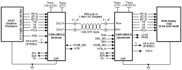
The DS90UB926Q-Q1 deserializer, in conjunction with the DS90UB925Q-Q1 serializer, provides a complete digital interface for concurrent transmission of high-speed video, audio, and control data for automotive display and image-sensing applications.
This chipset translates a parallel RGB video interface into a single-pair high-speed serialized interface. The serial bus scheme, FPD-Link III, supports full duplex of high-speed forward data transmission and low-speed backchannel communication over a single differential link. Consolidation of video data and control over a single differential pair reduces the interconnect size and weight, while also eliminating skew issues and simplifying system design.
The DS90UB926Q-Q1 deserializer recovers the RGB data, three video control signals, and four synchronized I2S audio signals. The device extracts the clock from a high-speed serial stream. An output LOCK pin provides the link status if the incoming data stream is locked, without the use of a training sequence or special SYNC patterns, as well as a reference clock.
PART NUMBER | PACKAGE | BODY SIZE (NOM) |
---|---|---|
DS90UB926Q-Q1 | WQFN (60) | 9.00 mm × 9.00 mm |
Changes from C Revision (February 2017) to D Revision
Changes from B Revision (January 2015) to C Revision
Changes from A Revision (April 2013) to B Revision
Changes from * Revision (July 2012) to A Revision
The DS90UB926Q-Q1 deserializer has a 31-bit parallel LVCMOS output interface to accommodate the RGB, video control, and audio data.
An adaptive equalizer optimizes the maximum cable reach. EMI is minimized by output SSC generation (SSCG) and enhanced progressive turnon (EPTO) features.
PIN | I/O, TYPE | DESCRIPTION | |
---|---|---|---|
NAME | NO. | ||
LVCMOS PARALLEL INTERFACE | |||
ROUT[23:0] / R[7:0], G[7:0], B[7:0] | 41, 40, 39, 37, 36, 35, 34, 33, 28, 27, 26, 25, 23, 22, 21, 20, 19, 18, 17, 14, 12, 11, 10, 9 | O, LVCMOS with pulldown |
Parallel Interface Data Output Pins Leave open if unused. ROUT0 / R0 can optionally be used as GPIO0 and ROUT1 / R1 can optionally be used as GPIO1. ROUT8 / G0 can optionally be used as GPIO2 and ROUT9 / G1 can optionally be used as GPIO3. ROUT16 / B0 can optionally be used as GPO_REG4 and ROUT17/ B1 can optionally be used as I2S_DB / GPO_REG5. |
HS | 8 | O, LVCMOS with pulldown |
Horizontal Sync Output Pin Video control signal pulse width must be 3 PCLKs or longer to be transmitted when the Control Signal Filter is enabled. There is no restriction on the minimum transition pulse when the Control Signal Filter is disabled. The signal is limited to 2 transitions per 130 PCLKs. See Table 11 |
VS | 7 | O, LVCMOS with pulldown |
Vertical Sync Output Pin Video control signal is limited to 1 transition per 130 PCLKs. Thus, the minimum pulse width is 130 PCLKs. |
DE | 6 | O, LVCMOS with pulldown |
Data Enable Output Pin Video control signal pulse width must be 3 PCLKs or longer to be transmitted when the Control Signal Filter is enabled. There is no restriction on the minimum transition pulse when the Control Signal Filter is disabled. The signal is limited to 2 transitions per 130 PCLKs. See Table 11 |
PCLK | 5 | O, LVCMOS with pulldown |
Pixel Clock Output Pin. Strobe edge set by RFB configuration register. See Table 11 |
I2S_CLK, I2S_WC, I2S_DA | 1, 30, 45 | O, LVCMOS with pulldown |
Digital Audio Interface Data Output Pins Leave open if unused I2S_CLK can optionally be used as GPO_REG8, I2S_WC can optionally be used as GPO_REG7, and I2S_DA can optionally be used as GPO_REG6. |
MCLK | 60 | O, LVCMOS with pulldown |
I2S Master Clock Output x1, x2, or x4 of I2S_CLK Frequency |
OPTIONAL PARALLEL INTERFACE | |||
I2S_DB | 18 | O, LVCMOS with pulldown |
Second Channel Digital Audio Interface Data Output pin at 18–bit color mode and set by MODE_SEL or configuration register Leave open if unused I2S_B can optionally be used as BI or GPO_REG5. |
GPIO[3:0] | 27, 28, 40, 41 | I/O, LVCMOS with pulldown |
Standard General Purpose IOs. Available only in 18-bit color mode, and set by MODE_SEL or configuration register. See Table 11 Leave open if unused Shared with G1, G0, R1 and R0. |
GPO_REG[8:4] | 1, 30, 45, 18, 19 | O, LVCMOS with pulldown |
General Purpose Outputs and set by configuration register. See Table 11
Shared with I2S_CLK, I2S_WC, I2S_DA, I2S_DB or B1, B0. |
INTB_IN | 16 | Input, LVCMOS with pulldown | Interrupt Input Shared with BISTC |
OPTIONAL PARALLEL INTERFACE | |||
PDB | 59 | I, LVCMOS with pulldown |
Power-down Mode Input Pin PDB = H, device is enabled (normal operation) Refer to Power Up Requirements and PDB Pin. PDB = L, device is powered down. When the device is in the POWER DOWN state, the LVCMOS Outputs are in TRI-STATE, the PLL is shutdown and IDD is minimized. . |
OEN | 31 | Input, LVCMOS with pulldown | Output Enable Pin See Table 8 |
OSS_SEL | 46 | Input, LVCMOS with pulldown | Output Sleep State Select Pin See Table 8 |
MODE_SEL | 15 | I, Analog | Device Configuration Select. See Table 9 |
IDx | 56 | I, Analog | I2C Serial Control Bus Device ID Address Select External pullup to VDD33 is required under all conditions, DO NOT FLOAT. Connect to external pullup and pulldown resistor to create a voltage divider. See Figure 23 |
SCL | 3 | I/O, LVCMOS Open-Drain |
I2C Clock Input / Output Interface Must have an external pullup to VDD33, DO NOT FLOAT. Recommended pullup: 4.7 kΩ. |
SDA | 2 | I/O, LVCMOS Open-Drain |
I2C Data Input / Output Interface Must have an external pullup to VDD33, DO NOT FLOAT. Recommended pullup: 4.7 kΩ. |
BISTEN | 44 | I, LVCMOS with pulldown | BIST Enable Pin 0: BIST Mode is disabled. 1: BIST Mode is enabled. |
BISTC | 16 | I, LVCMOS with pulldown | BIST Clock Select Shared with INTB_IN 0: PCLK; 1: 33 MHz |
STATUS | |||
LOCK | 32 | O, LVCMOS with pulldown | LOCK Status Output Pin 0: PLL is unlocked, ROUT[23:0]/RGB[7:0], I2S[2:0], HS, VS, DE and PCLK output states are controlled by OEN. May be used as Link Status or Display Enable 1: PLL is Locked, outputs are active |
PASS | 42 | O, LVCMOS with pulldown | PASS Output Pin 0: One or more errors were detected in the received payload 1: ERROR FREE Transmission Leave Open if unused. Route to test point (pad) recommended |
FPD-LINK III SERIAL INTERFACE | |||
RIN+ | 49 | I, LVDS | True Input. The interconnection should be AC-coupled to this pin with a 0.1-μF capacitor. |
RIN- | 50 | I, LVDS | Inverting Input. The interconnection should be AC-coupled to this pin with a 0.1-μF capacitor. |
CMLOUTP | 52 | O, LVDS | True CML Output Monitor point for equalized differential signal |
CMLOUTN | 53 | O, LVDS | Inverting CML Output Monitor point for equalized differential signal |
CMF | 51 | Analog | Common Mode Filter. Connect 0.1-μF capacitor to GND |
POWER AND GROUND(1) | |||
VDD33_A, VDD33_B | 48, 29 | Power | Power to on-chip regulator 3 V – 3.6 V. Requires 4.7 µF to GND at each VDD pin. |
VDDIO | 13, 24, 38 | Power | LVCMOS I/O Power 1.8 V ±5% OR 3 V – 3.6 V. Requires 4.7 µF to GND at each VDDIO pin. |
GND | DAP | Ground | DAP is the large metal contact at the bottom side, located at the center of the WQFN package. Connect to the ground plane (GND) with at least 9 vias. |
REGULATOR CAPACITOR | |||
CAPR12, CAPP12, CAPI2S | 55, 57, 58 | CAP | Decoupling capacitor connection for on-chip regulator. Requires a 4.7 µF to GND at each CAP pin. |
CAPL12 | 4 | CAP | Decoupling capacitor connection for on-chip regulator. Requires two 4.7 µF to GND at this CAP pin. |
OTHERS | |||
NC | 54 | NC | No connect. This pin may be left open or tied to any level. |
RES[1:0] | 43.47 | GND | Reserved - tie to Ground. |
MIN | MAX | UNIT | ||
---|---|---|---|---|
Supply voltage – VDD33 | −0.3 | 4 | V | |
Supply voltage – VDDIO | −0.3 | 4 | V | |
LVCMOS I/O voltage | −0.3 | (VDDIO + 0.3) | V | |
Deserializer input voltage | −0.3 | 2.75 | V | |
Junction temperature | 150 | °C | ||
Maximum power dissipation capacity at 25°C | RθJA | 31 | °C/W | |
RθJC | 2.4 | °C/W | ||
Storage temperature, Tstg | −65 | 150 | °C |
VALUE | UNIT | ||||
---|---|---|---|---|---|
V(ESD) | Electrostatic discharge | Human-body model (HBM), per AEC Q100-002(1) | ±8000 | V | |
Charged-device model (CDM), per AEC Q100-011 | ±1250 | ||||
Machine model | ±250 | ||||
(IEC, powered-up only) RD = 330 Ω, CS = 150 pF |
Air Discharge (Pin 49 and 50) | ±15000 | |||
Contact Discharge (Pin 49 and 50) | ±8000 | ||||
(ISO1060SN5), RD = 330 Ω CS = 150 pF |
Air Discharge (Pin 49 and 50) | ±15000 | |||
Contact Discharge (Pin 49 and 50) | ±8000 | ||||
(ISO10605), RD = 2 kΩ CS = 150 and 330 pF |
Air Discharge (Pin 49 and 50) | ±15000 | |||
Contact Discharge (Pin 49 and 50) | ±8000 |
MIN | NOM | MAX | UNIT | ||
---|---|---|---|---|---|
Supply voltage (VDD33) | 3 | 3.3 | 3.6 | V | |
LVCMOS supply voltage (VDDIO) | Connect VDDIO to 3.3 V and use 3.3-V IOs | 3 | 3.3 | 3.6 | V |
Connect VDDIO to 1.8 V and use 1.8-V IOs | 1.71 | 1.8 | 1.89 | V | |
Operating free air temperature (TA) | −40 | 25 | 105 | °C | |
PCLK frequency | 5 | 85 | MHz | ||
Supply noise(1) | 100 | mVP-P |
THERMAL METRIC(1) | DS90UB926Q-Q1 | UNIT | |
---|---|---|---|
NKB (WQFN) | |||
60 PINS | |||
RθJA | Junction-to-ambient thermal resistance | 26.2 | °C/W |
RθJC(top) | Junction-to-case (top) thermal resistance | 8.1 | °C/W |
RθJB | Junction-to-board thermal resistance | 5.2 | °C/W |
ψJT | Junction-to-top characterization parameter | 0.1 | °C/W |
ψJB | Junction-to-board characterization parameter | 5.2 | °C/W |
RθJC(bot) | Junction-to-case (bottom) thermal resistance | 1.1 | °C/W |
PARAMETER | TEST CONDITIONS | PIN/FREQ. | MIN | TYP | MAX | UNIT | ||
---|---|---|---|---|---|---|---|---|
LVCMOS I/O DC SPECIFICATIONS | ||||||||
VIH | High Level Voltage | VDDIO = 3 to 3.6 V | PDB | 2 | VDDIO | V | ||
VIL | Low Level Input | VDDIO = 3 to 3.6 V | GND | 0.8 | V | |||
IIN | Input Current | VIN = 0 V or VDDIO = 3 to 3.6 V | –10 | ±1 | 10 | µA | ||
VIH | High Level Input Voltage | VDDIO = 3 to 3.6 V | OEN, OSS_SEL, BISTEN, BISTC / INTB_IN, GPIO[3:0] | 2 | VDDIO | V | ||
VDDIO = 1.71 to 1.89 V | 0.65 × VDDIO |
VDDIO | ||||||
VIL | Low Level Input Voltage | VDDIO = 3 to 3.6 V | GND | 0.8 | V | |||
VDDIO = 1.71 to 1.89 V | GND | 0.35 × VDDIO |
||||||
IIN | Input Current | VIN = 0 V or VDDIO | VDDIO = 3 to 3.6 V |
−10 | ±1 | 10 | μA | |
VDDIO = 1.7 to 1.89 V |
−10 | ±1 | 10 | |||||
VOH | High Level Output Voltage | IOH = −4 mA | VDDIO = 3 to 3.6 V | ROUT[23:0], HS, VS, DE, PCLK, LOCK, PASS, MCLK, I2S_CLK, I2S_WC, I2S_DA, I2S_DB, GPO_REG[8:4] | 2.4 | VDDIO | V | |
VDDIO = 1.7 to 1.89 V |
VDDIO – 0.45 | VDDIO | ||||||
VOL | Low Level Output Voltage | IOL = 4 mA | VDDIO = 3 to 3.6 V | GND | 0.4 | V | ||
VDDIO = 1.7 to 1.89 V |
GND | 0.35 | ||||||
IOS | Output Short Circuit Current | VOUT = 0 V | −60 | mA | ||||
IOZ | Tri-state Output Current | VOUT = 0 V or VDDIO, PDB = L | −10 | 10 | μA | |||
FPD-LINK III CML RECEIVER INPUT DC SPECIFICATIONS | ||||||||
VTH | Differential Threshold High Voltage | VCM = 2.5 V (Internal VBIAS) |
RIN+, RIN– | 50 | mV | |||
VTL | Differential Threshold Low Voltage | −50 | mV | |||||
VCM | Differential Common-mode Voltage | 1.8 | V | |||||
RT | Internal Termination Resistor - Differential | 80 | 100 | 120 | Ω | |||
CML MONITOR DRIVER OUTPUT DC SPECIFICATIONS | ||||||||
VODp-p | Differential Output Voltage | RL = 100 Ω | CMLOUTP, CMLOUTN | 360 | mVp-p | |||
SUPPLY CURRENT | ||||||||
IDD1 | Supply Current (includes load current) f = 85 MHz |
CL = 12 pF, Checker Board Pattern (Figure 1) |
VDD33= 3.6 V | VDD33 | 125 | 145 | mA | |
IDDIO1 | VDDIO= 3.6 V | VDDIO | 110 | 118 | mA | |||
VDDIO = 1.89 V | 60 | 75 | ||||||
IDD2 | Supply Current (includes load current) f = 85MHz |
CL = 4 pF Checker Board Pattern (Figure 1) |
VDD33 = 3.6 V | VDD33 | 125 | 145 | mA | |
IDDIO2 | VDDIO = 3.6 V | VDDIO | 75 | 85 | mA | |||
VDDIO = 1.89 V | 50 | 65 | ||||||
IDDS | Supply Current Sleep Mode | Without Input Serial Stream | VDD33 = 3.6 V | VDD33 | 90 | 115 | mA | |
IDDIOS | VDDIO = 3.6 V | VDDIO | 3 | 5 | mA | |||
VDDIO = 1.89 V | 2 | 3 | ||||||
IDDZ | Supply Current Power Down | PDB = L, All LVCMOS inputs are floating or tied to GND | VDD33 = 3.6 V | VDD33 | 2 | 10 | mA | |
IDDIOZ | VDDIO = 3.6 V | VDDIO | 0.05 | 10 | mA | |||
VDDIO = 1.89 V | 0.05 | 10 |
PARAMETER | TEST CONDITIONS | PIN/FREQ. | MIN | TYP | MAX | UNIT | |
---|---|---|---|---|---|---|---|
GPIO BIT RATE | |||||||
BR | Forward Channel Bit Rate | See(5)(6) | f = 5 to 85 MHz, GPIO[3:0] |
0.25 × f | Mbps | ||
Back Channel Bit Rate | >50 | >75 | kbps | ||||
CML MONITOR DRIVER OUTPUT AC SPECIFICATIONS | |||||||
EW | Differential Output Eye Opening Width(4) | RL = 100 Ω, Jitter Freq > f / 40 (Figure 2)(5)(6) |
CMLOUTP, CMLOUTN, f = 85 MHz |
0.3 | 0.4 | UI | |
EH | Differential Output Eye Height | 200 | 300 | mV | |||
BIST MODE | |||||||
tPASS | BIST PASS Valid Time BISTEN = H (Figure 8)(5)(6) |
PASS | 800 | ns | |||
SSCG MODE | |||||||
fDEV | Spread Spectrum Clocking Deviation Frequency | See Figure 14, Table 1, Table 2 (5) (6) | f = 85 MHz, SSCG = ON |
±0.5% | ±2.5% | ||
fMOD | Spread Spectrum Clocking Modulation Frequency | 8 | 100 | kHz |
PARAMETER | TEST CONDITIONS | MIN | TYP | MAX | UNIT | |
---|---|---|---|---|---|---|
VIH | Input High Level | SDA and SCL | 0.7 × VDD33 |
VDD33 | V | |
VIL | Input Low Level Voltage | SDA and SCL | GND | 0.3 × VDD33 |
V | |
VHY | Input Hysteresis | > 50 | mV | |||
VOL | SDA, IOL = 1.25 mA | 0 | 0.36 | V | ||
Iin | SDA or SCL, VIN = VDD33 or GND | –10 | 10 | µA | ||
tR | SDA RiseTime – READ | SDA, RPU = 10 kΩ, Cb ≤ 400 pF (Figure 9) | 430 | ns | ||
tF | SDA Fall Time – READ | 20 | ns | |||
tSU;DAT | Setup Time — READ | See Figure 9 | 560 | ns | ||
tHD;DAT | Holdup Time — READ | See Figure 9 | 615 | ns | ||
tSP | Input Filter | 50 | ns | |||
Cin | Input Capacitance | SDA or SCL | < 5 | pF |
MIN | NOM | MAX | UNIT | |||
---|---|---|---|---|---|---|
tR | SDA RiseTime – READ | SDA, RPU = 10 kΩ, Cb ≤ 400 pF (Figure 9) | 430 | ns | ||
tF | SDA Fall Time – READ | 20 | ns | |||
tSU;DAT | Setup Time — READ | See Figure 9 | 560 | ns | ||
tHD;DAT | Holdup Time — READ | See Figure 9 | 615 | ns | ||
tSP | Input Filter | 50 | ns |
MIN | NOM | MAX | UNIT | |||
---|---|---|---|---|---|---|
fSCL | SCL Clock Frequency | Standard Mode | 0 | 100 | kHz | |
Fast Mode | 0 | 400 | kHz | |||
tLOW | SCL Low Period | Standard Mode | 4.7 | µs | ||
Fast Mode | 1.3 | µs | ||||
tHIGH | SCL High Period | Standard Mode | 4 | µs | ||
Fast Mode | 0.6 | µs | ||||
tHD;STA | Hold time for a start or a repeated start condition (Figure 9) | Standard Mode | 4 | µs | ||
Fast Mode | 0.6 | µs | ||||
tSU:STA | Setup time for a start or a repeated start condition (Figure 9) | Standard Mode | 4.7 | µs | ||
Fast Mode | 0.6 | µs | ||||
tHD;DAT | Data Hold Time (Figure 9) | Standard Mode | 0 | 3.45 | µs | |
Fast Mode | 0 | 0.9 | µs | |||
tSU;DAT | Data Setup Time (Figure 9) | Standard Mode | 250 | ns | ||
Fast Mode | 100 | ns | ||||
tSU;STO | Setup Time for STOP Condition (Figure 9) | Standard Mode | 4 | µs | ||
Fast Mode | 0.6 | µs | ||||
tBUF | Bus Free Time between STOP and START (Figure 9) | Standard Mode | 4.7 | µs | ||
Fast Mode | 1.3 | µs | ||||
tr | SCL and SDA Rise Time (Figure 9) | Standard Mode | 1000 | ns | ||
Fast Mode | 300 | ns | ||||
tf | SCL and SDA Fall Time (Figure 9) | Standard Mode | 300 | ns | ||
Fast mode | 300 | ns |
PARAMETER | TEST CONDITIONS | PIN/FREQ. | MIN | TYP | MAX | UNIT | |
---|---|---|---|---|---|---|---|
tRCP | PCLK Output Period | tRCP = tTCP | PCLK | 11.76 | T | 200 | ns |
tRDC | PCLK Output Duty Cycle | 45% | 50% | 55% | |||
tCLH | LVCMOS Low-to-High Transition Time (Figure 3) | VDDIO = 1.71 to 1.89 V, CL = 12 pF |
ROUT[23:0], HS, VS, DE, PCLK, LOCK, PASS, MCLK, I2S_CLK, I2S_WC, I2S_DA, I2S_DB | 2 | 3 | ns | |
VDDIO = 3 to 3.6 V, CL = 12 pF |
2 | 3 | ns | ||||
tCHL | LVCMOS High-to-Low Transition Time (Figure 3) | VDDIO = 1.71 to 1.89 V, CL = 12 pF |
2 | 3 | ns | ||
VDDIO = 3 to 3.6 V, CL = 12 pF |
2 | 3 | ns | ||||
tROS | Data Valid before PCLK – Setup Time SSCG = OFF (Figure 6) |
VDDIO = 1.71 to 1.89 V, CL = 12 pF |
2.2 | ns | |||
VDDIO = 3 to 3.6 V, CL = 12 pF |
2.2 | ns | |||||
tROH | Data Valid after PCLK – Hold Time SSCG = OFF (Figure 6) |
VDDIO = 1.71 to 1.89 V, CL = 12 pF |
3 | ns | |||
VDDIO = 3 to 3.6 V, CL = 12 pF |
3 | ns | |||||
tXZR | Active to OFF Delay (Figure 5)(1) (2) | OEN = L, OSS_SEL = H | ROUT[23:0] | 10 | ns | ||
HS, VS, DE, PCLK, LOCK, PASS | 15 | ns | |||||
MCLK, I2S_CLK, I2S_WC, I2S_DA, I2S_DB | 60 | ns | |||||
tDDLT | Lock Time (Figure 5)(1)(2)(3) | SSCG = OFF | f = 5 to 85MHz | 5 | 40 | ns | |
tDD | Delay – Latency(1)(2) | f = 5 to 85MHz | 147*T | ns | |||
tDCCJ | Cycle-to-Cycle Jitter(1)(2) | SSCG = OFF | f = 5 to <15 MHz | 0.5 | ns | ||
f = 15 to 85 MHz | 0.2 | ns | |||||
I2S_CLK = 1 to 12.28MHz | ±2 | ns | |||||
tONS | Data Valid After OEN = H SetupTime (Figure 7)(1)(2) | VDDIO = 1.71 to 1.89 V, CL = 12 pF |
ROUT[23:0], HS, VS, DE, PCLK, MCLK, I2S_CLK, I2S_WC, I2S_DA, I2S_DB | 50 | ns | ||
VDDIO = 3 to 3.6 V, CL = 12 pF |
50 | ns | |||||
tONH | Data Tri-State After OEN = L SetupTime (Figure 7)(1)(2) | VDDIO = 1.71 to 1.89 V, CL = 12 pF |
50 | ns | |||
VDDIO = 3 to 3.6 V, CL = 12 pF |
50 | ns | |||||
tSES | Data Tri-State after OSS_ SEL = H, Setup Time (Figure 7)(1)(2) | VDDIO = 1.71 to 1.89 V, CL = 12 pF |
5 | ns | |||
VDDIO = 3 to 3.6 V, CL = 12 pF |
5 | ns | |||||
tSEH | Data to Low after OSS_SEL = L Setup Time (Figure 7)(1)(2) | VDDIO = 1.71 to 1.89 V, CL = 12 pF |
5 | ns | |||
VDDIO = 3 to 3.6 V, CL = 12 pF |
5 | ns |
Note: On the rising edge of each clock period, the CML driver outputs a low Stop bit, high Start bit, and 33 DC-scrambled data bits. | ||