SNLS477D October 2014 – February 2022 DS90UB948-Q1
PRODUCTION DATA
- 1 Features
- 2 Applications
- 3 Description
- 4 Revision History
- 5 Pin Configuration and Functions
-
6 Specifications
- 6.1 Absolute Maximum Ratings
- 6.2 ESD Ratings
- 6.3 Recommended Operating Conditions
- 6.4 Thermal Information
- 6.5 DC Electrical Characteristics
- 6.6 AC Electrical Characteristics
- 6.7 Timing Requirements for the Serial Control Bus
- 6.8 Switching Characteristics
- 6.9 Timing Diagrams and Test Circuits
- 6.10 Typical Characteristics
-
7 Detailed Description
- 7.1 Overview
- 7.2 Functional Block Diagram
- 7.3
Feature Description
- 7.3.1 High-Speed Forward Channel Data Transfer
- 7.3.2 Low-Speed Back Channel Data Transfer
- 7.3.3 FPD-Link III Port Register Access
- 7.3.4 Oscillator Output
- 7.3.5 Clock and Output Status
- 7.3.6 LVCMOS VDDIO Option
- 7.3.7 Power Down (PDB)
- 7.3.8 Interrupt Pin — Functional Description and Usage (INTB_IN)
- 7.3.9 General-Purpose I/O (GPIO)
- 7.3.10 SPI Communication
- 7.3.11 Backward Compatibility
- 7.3.12 Adaptive Equalizer
- 7.3.13 I2S Audio Interface
- 7.3.14 Repeater
- 7.3.15 Built-In Self Test (BIST)
- 7.3.16 Internal Pattern Generation
- 7.4
Device Functional Modes
- 7.4.1
Configuration Select MODE_SEL[1:0]
- 7.4.1.1 1-Lane FPD-Link III Input, Single Link OpenLDI Output
- 7.4.1.2 1-Lane FPD-Link III Input, Dual Link OpenLDI Output
- 7.4.1.3 2-Lane FPD-Link III Input, Dual Link OpenLDI Output
- 7.4.1.4 2-Lane FPD-Link III Input, Single Link OpenLDI Output
- 7.4.1.5 1-Lane FPD-Link III Input, Single Link OpenLDI Output (Replicate)
- 7.4.2 MODE_SEL[1:0]
- 7.4.3 OpenLDI Output Frame and Color Bit Mapping Select
- 7.4.1
Configuration Select MODE_SEL[1:0]
- 7.5 Image Enhancement Features
- 7.6
Programming
- 7.6.1 Serial Control Bus
- 7.6.2 Multi-Controller Arbitration Support
- 7.6.3 I2C Restrictions on Multi-Controller Operation
- 7.6.4 Multi-Controller Access to Device Registers for Newer FPD-Link III Devices
- 7.6.5 Multi-Controller Access to Device Registers for Older FPD-Link III Devices
- 7.6.6 Restrictions on Control Channel Direction for Multi-Controller Operation
- 7.7 Register Maps
- 8 Application and Implementation
- 9 Power Supply Recommendations
- 10Layout
- 11Device and Documentation Support
- 12Mechanical, Packaging, and Orderable Information
Package Options
Mechanical Data (Package|Pins)
- NKD|64
Thermal pad, mechanical data (Package|Pins)
- NKD|64
Orderable Information
7.5.4 Adaptive Hi-FRC Dithering
The adaptive frame rate control FRC dithering feature delivers product-differentiating image quality. It reduces 24-bit RGB (8 bits per sub-pixel) to 18-bit RGB (6 bits per sub-pixel), smoothing color gradients, and allowing the flexibility to use lower cost 18-bit displays. FRC dithering is a method to emulate missing colors on a lower color depth LCD display by changing the pixel color slightly with every frame. FRC is achieved by controlling on and off pixels over multiple frames (temporal). Static dithering regulates the number of on and off pixels in a small defined pixel group (spatial). The FRC module includes both temporal and spatial methods and also Hi-FRC. Conventional FRC can display only 16,194,277 colors with 6-bit RGB source. Hi-FRC enables full (16,777,216) color on an 18-bit LCD panel. The adaptive FRC module also includes input pixel detection to apply specific Spatial dithering methods for smoother gray level transitions. When enabled, the lower LSBs of each RGB output are not active; only 18-bit data (6 bits per R,G and B) are driven to the display. This feature is enabled via serial control bus register. Two FRC functional blocks are available, and may be independently enabled. FRC1 precedes the white-balance LUT, and is intended to be used when 24-bit data is being driven to an 18-bit display with a white-balance LUT that is calibrated for an 18-bit data source. The second FRC block, RC2, follows the white balance block and is intended to be used when fine adjustment of color temperature is required on an 18-bit color display, or when a 24-bit source drives an 18-bit display with a white-balance LUT calibrated for 24-bit source data.
For proper operation of the FRC dithering feature, the user must provide a description of the display timing control signals. The timing mode, sync mode (HS, VS) or DE only must be specified, along with the active polarity of the timing control signals. All this information is entered to device control registers via the serial bus interface.
Adaptive Hi-FRC dithering consists of several components. Initially, the incoming 8-bit data is expanded to 9-bit data. This allows the effective dithered result to support a total of 16.7 million colors. The incoming 9-bit data is evaluated, and one of four possible algorithms is selected. The majority of incoming data sequences are supported by the default dithering algorithm. Certain incoming data patterns (black/white pixel, full on/off sub-pixel) require special algorithms designed to eliminate visual artifacts associated with these specific gray level transitions. Three algorithms are defined to support these critical transitions.
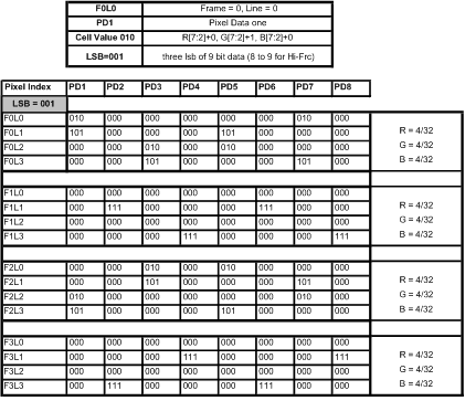
An example of the default dithering algorithm is shown in Figure 7-27. The 1 or 0 value shown in Figure 7-27
Figure 7-27 describes whether the 6-bit value is increased by 1 (“1”) or left unchanged (“0”). In this case, the 3 truncated LSBs are 001.
 Figure 7-27 Default FRC Algorithm