SNLS650 May 2019 DS90UB949A-Q1
PRODUCTION DATA.
- 1 Features
- 2 Applications
- 3 Description
- 4 Revision History
- 5 Pin Configuration and Functions
-
6 Specifications
- 6.1 Absolute Maximum Ratings
- 6.2 ESD Ratings
- 6.3 Recommended Operating Conditions
- 6.4 Thermal Information
- 6.5 DC Electrical Characteristics
- 6.6 AC Electrical Characteristics
- 6.7 DC and AC Serial Control Bus Characteristics
- 6.8 Recommended Timing for the Serial Control Bus
- 6.9 Timing Diagrams
- 6.10 Typical Characteristics
-
7 Detailed Description
- 7.1 Overview
- 7.2 Functional Block Diagram
- 7.3
Feature Description
- 7.3.1 High-Definition Multimedia Interface (HDMI)
- 7.3.2 Transition Minimized Differential Signaling
- 7.3.3 Enhanced Display Data Channel
- 7.3.4 Extended Display Identification Data (EDID)
- 7.3.5 Consumer Electronics Control (CEC)
- 7.3.6 +5-V Power Signal
- 7.3.7 Hot Plug Detect (HPD)
- 7.3.8 High-Speed Forward Channel Data Transfer
- 7.3.9 Back Channel Data Transfer
- 7.3.10 FPD-Link III Port Register Access
- 7.3.11 Power Down (PDB)
- 7.3.12 Serial Link Fault Detect
- 7.3.13 Interrupt Pin (INTB)
- 7.3.14 Remote Interrupt Pin (REM_INTB)
- 7.3.15 General-Purpose I/O
- 7.3.16 SPI Communication
- 7.3.17 Backward Compatibility
- 7.3.18 Audio Modes
- 7.3.19 Built-In Self Test (BIST)
- 7.3.20 Internal Pattern Generation
- 7.3.21 Spread-Spectrum Clock Tolerance
- 7.4 Device Functional Modes
- 7.5
Programming
- 7.5.1 Serial Control Bus
- 7.5.2 Multi-Master Arbitration Support
- 7.5.3 I2C Restrictions on Multi-Master Operation
- 7.5.4 Multi-Master Access to Device Registers for Newer FPD-Link III Devices
- 7.5.5 Multi-Master Access to Device Registers for Older FPD-Link III Devices
- 7.5.6 Restrictions on Control Channel Direction for Multi-Master Operation
- 7.5.7 Prevention of I2C Faults During Abrupt System Faults
- 7.6 Register Maps
- 8 Application and Implementation
- 9 Power Supply Recommendations
- 10Layout
- 11Device and Documentation Support
- 12Mechanical, Packaging, and Orderable Information
Package Options
Mechanical Data (Package|Pins)
- RGC|64
Thermal pad, mechanical data (Package|Pins)
- RGC|64
Orderable Information
7.3.19.2 Forward-Channel and Back-Channel Error Checking
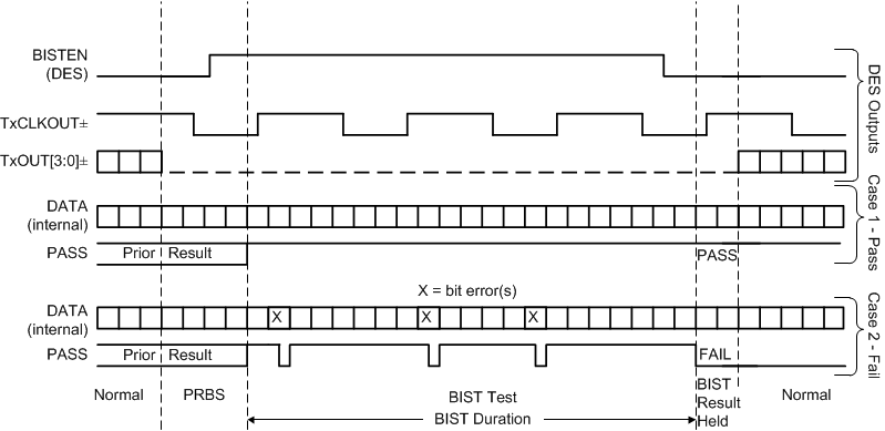
While in BIST mode, the serializer stops sampling the FPD-Link input pins and switches over to an internal, all-zeroes pattern. The internal, all-zeroes pattern goes through the scrambler, DC balancing, and so forth, and is transmitted over the serial link to the deserializer. The deserializer, on locking to the serial stream, compares the recovered serial stream with all zeroes and records any errors in status registers. Errors are also dynamically reported on the PASS pin of the deserializer.
The back channel data is checked for CRC errors once the serializer locks onto the back channel serial stream, as indicated by link detect status (register bit 0x0C[0] - Table 10). CRC errors are recorded in an 8-bit register in the deserializer. The register is cleared when the serializer enters BIST mode. As soon as the serializer enters BIST mode, the functional mode CRC register starts recording any back channel CRC errors. The BIST mode CRC error register is active in BIST mode only and keeps a record of the last BIST run until the register is cleared or the serializer enters BIST mode again.
 Figure 19. BIST Waveforms in Conjunction With Deserializer Signals