SNLS455A November   2014  – March 2019 DS90UH947-Q1

PRODUCTION DATA.  

  1. Features
  2. Applications
  3. Description
    1.     Device Images
      1.      Applications Diagram
  4. Revision History
  5. Pin Configuration and Functions
    1.     Pin Functions
  6. Specifications
    1. 6.1  Absolute Maximum Ratings
    2. 6.2  ESD Ratings
    3. 6.3  Recommended Operating Conditions
    4. 6.4  Thermal Information
    5. 6.5  DC Electrical Characteristics
    6. 6.6  AC Electrical Characteristics
    7. 6.7  DC and AC Serial Control Bus Characteristics
    8. 6.8  Recommended Timing for the Serial Control Bus
    9. 6.9  Timing Diagrams
    10. 6.10 Typical Characteristics
  7. Detailed Description
    1. 7.1 Overview
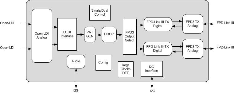
    2. 7.2 Functional Block Diagram
    3. 7.3 Feature Description
      1. 7.3.1  High-Speed Forward Channel Data Transfer
      2. 7.3.2  Back Channel Data Transfer
      3. 7.3.3  FPD-Link III Port Register Access
      4. 7.3.4  OpenLDI Input Frame and Color Bit Mapping Select
      5. 7.3.5  Video Control Signals
      6. 7.3.6  Power Down (PDB)
      7. 7.3.7  Serial Link Fault Detect
      8. 7.3.8  Interrupt Pin (INTB)
      9. 7.3.9  Remote Interrupt Pin (REM_INTB)
      10. 7.3.10 General-Purpose I/O
        1. 7.3.10.1 GPIO[3:0] Configuration
        2. 7.3.10.2 Back Channel Configuration
        3. 7.3.10.3 GPIO_REG[8:5] Configuration
      11. 7.3.11 SPI Communication
        1. 7.3.11.1 SPI Mode Configuration
        2. 7.3.11.2 Forward Channel SPI Operation
        3. 7.3.11.3 Reverse Channel SPI Operation
      12. 7.3.12 Backward Compatibility
      13. 7.3.13 Audio Modes
        1. 7.3.13.1 I2S Audio Interface
          1. 7.3.13.1.1 I2S Transport Modes
          2. 7.3.13.1.2 I2S Repeater
        2. 7.3.13.2 TDM Audio Interface
      14. 7.3.14 HDCP Repeater
        1. 7.3.14.1 HDCP
        2. 7.3.14.2 HDCP Repeater
          1. 7.3.14.2.1 Repeater Configuration
          2. 7.3.14.2.2 Repeater Connections
            1. 7.3.14.2.2.1 Repeater Fan-Out Electrical Requirements
            2. 7.3.14.2.2.2 HDCP I2S Audio Encryption
      15. 7.3.15 Built-In Self Test (BIST)
        1. 7.3.15.1 BIST Configuration and Status
        2. 7.3.15.2 Forward Channel and Back Channel Error Checking
      16. 7.3.16 Internal Pattern Generation
        1. 7.3.16.1 Pattern Options
        2. 7.3.16.2 Color Modes
        3. 7.3.16.3 Video Timing Modes
        4. 7.3.16.4 External Timing
        5. 7.3.16.5 Pattern Inversion
        6. 7.3.16.6 Auto Scrolling
        7. 7.3.16.7 Additional Features
    4. 7.4 Device Functional Modes
      1. 7.4.1 Mode Select Configuration Settings (MODE_SEL[1:0])
      2. 7.4.2 FPD-Link III Modes of Operation
        1. 7.4.2.1 Single Link Operation
        2. 7.4.2.2 Dual Link Operation
        3. 7.4.2.3 Replicate Mode
        4. 7.4.2.4 Auto-Detection of FPD-Link III Modes
    5. 7.5 Programming
      1. 7.5.1 Serial Control Bus
      2. 7.5.2 Multi-Master Arbitration Support
      3. 7.5.3 I2C Restrictions on Multi-Master Operation
      4. 7.5.4 Multi-Master Access to Device Registers for Newer FPD-Link III Devices
      5. 7.5.5 Multi-Master Access to Device Registers for Older FPD-Link III Devices
      6. 7.5.6 Restrictions on Control Channel Direction for Multi-Master Operation
    6. 7.6 Register Maps
  8. Application and Implementation
    1. 8.1 Applications Information
    2. 8.2 Typical Applications
      1. 8.2.1 Design Requirements
      2. 8.2.2 Detailed Design Procedure
        1. 8.2.2.1 High-Speed Interconnect Guidelines
      3. 8.2.3 Application Curves
        1. 8.2.3.1 Application Performance Plots
  9. Power Supply Recommendations
    1. 9.1 Power-Up Requirements and PDB Pin
  10. 10Layout
    1. 10.1 Layout Guidelines
    2. 10.2 Layout Example
  11. 11Device and Documentation Support
    1. 11.1 Documentation Support
      1. 11.1.1 Related Documentation
    2. 11.2 Trademarks
    3. 11.3 Electrostatic Discharge Caution
    4. 11.4 Glossary
  12. 12Mechanical, Packaging and Orderable Information

Package Options

Mechanical Data (Package|Pins)
Thermal pad, mechanical data (Package|Pins)
Orderable Information

Functional Block Diagram

DS90UH947-Q1 UH947_BlockDia.gif