SNLS455A November 2014 – March 2019 DS90UH947-Q1
PRODUCTION DATA.
- 1 Features
- 2 Applications
- 3 Description
- 4 Revision History
- 5 Pin Configuration and Functions
-
6 Specifications
- 6.1 Absolute Maximum Ratings
- 6.2 ESD Ratings
- 6.3 Recommended Operating Conditions
- 6.4 Thermal Information
- 6.5 DC Electrical Characteristics
- 6.6 AC Electrical Characteristics
- 6.7 DC and AC Serial Control Bus Characteristics
- 6.8 Recommended Timing for the Serial Control Bus
- 6.9 Timing Diagrams
- 6.10 Typical Characteristics
-
7 Detailed Description
- 7.1 Overview
- 7.2 Functional Block Diagram
- 7.3
Feature Description
- 7.3.1 High-Speed Forward Channel Data Transfer
- 7.3.2 Back Channel Data Transfer
- 7.3.3 FPD-Link III Port Register Access
- 7.3.4 OpenLDI Input Frame and Color Bit Mapping Select
- 7.3.5 Video Control Signals
- 7.3.6 Power Down (PDB)
- 7.3.7 Serial Link Fault Detect
- 7.3.8 Interrupt Pin (INTB)
- 7.3.9 Remote Interrupt Pin (REM_INTB)
- 7.3.10 General-Purpose I/O
- 7.3.11 SPI Communication
- 7.3.12 Backward Compatibility
- 7.3.13 Audio Modes
- 7.3.14 HDCP Repeater
- 7.3.15 Built-In Self Test (BIST)
- 7.3.16 Internal Pattern Generation
- 7.4 Device Functional Modes
- 7.5
Programming
- 7.5.1 Serial Control Bus
- 7.5.2 Multi-Master Arbitration Support
- 7.5.3 I2C Restrictions on Multi-Master Operation
- 7.5.4 Multi-Master Access to Device Registers for Newer FPD-Link III Devices
- 7.5.5 Multi-Master Access to Device Registers for Older FPD-Link III Devices
- 7.5.6 Restrictions on Control Channel Direction for Multi-Master Operation
- 7.6 Register Maps
- 8 Application and Implementation
- 9 Power Supply Recommendations
- 10Layout
- 11Device and Documentation Support
- 12Mechanical, Packaging and Orderable Information
Package Options
Mechanical Data (Package|Pins)
- RGC|64
Thermal pad, mechanical data (Package|Pins)
- RGC|64
Orderable Information
7.3.4 OpenLDI Input Frame and Color Bit Mapping Select
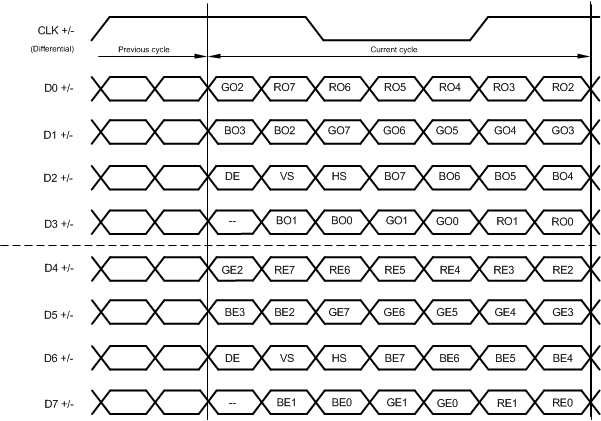
The DS90UH947-Q1 can be configured to accept 24-bit color (8-bit RGB) with 2 different mapping schemes, shown in Figure 13 and Figure 14. Each frame corresponds to a single pixel clock (PCLK) cycle. The LVDS clock input to CLK± follows a 4:3 duty cycle scheme, with each 28-bit pixel frame starting with two LVDS bit clock periods high, three low, and ending with two high. The mapping scheme is controlled by MAPSEL strap option or by Register (Table 10).
 Figure 13. 24-Bit Color Dual Pixel Mapping: MSBs on D3/D7 (OpenLDI Mapping)
  Figure 14. 24-Bit Color Dual Pixel Mapping: LSBs on D3/D7 (SPWG Mapping)
  Figure 15. 24-Bit Color Single Pixel Mapping: MSBs on D3 (OpenLDI Mapping)
  Figure 16. 24-Bit Color Single Pixel Mapping: LSBs on D3 (SPWG Mapping)