SNLS455A November 2014 – March 2019 DS90UH947-Q1
PRODUCTION DATA.
- 1 Features
- 2 Applications
- 3 Description
- 4 Revision History
- 5 Pin Configuration and Functions
-
6 Specifications
- 6.1 Absolute Maximum Ratings
- 6.2 ESD Ratings
- 6.3 Recommended Operating Conditions
- 6.4 Thermal Information
- 6.5 DC Electrical Characteristics
- 6.6 AC Electrical Characteristics
- 6.7 DC and AC Serial Control Bus Characteristics
- 6.8 Recommended Timing for the Serial Control Bus
- 6.9 Timing Diagrams
- 6.10 Typical Characteristics
-
7 Detailed Description
- 7.1 Overview
- 7.2 Functional Block Diagram
- 7.3
Feature Description
- 7.3.1 High-Speed Forward Channel Data Transfer
- 7.3.2 Back Channel Data Transfer
- 7.3.3 FPD-Link III Port Register Access
- 7.3.4 OpenLDI Input Frame and Color Bit Mapping Select
- 7.3.5 Video Control Signals
- 7.3.6 Power Down (PDB)
- 7.3.7 Serial Link Fault Detect
- 7.3.8 Interrupt Pin (INTB)
- 7.3.9 Remote Interrupt Pin (REM_INTB)
- 7.3.10 General-Purpose I/O
- 7.3.11 SPI Communication
- 7.3.12 Backward Compatibility
- 7.3.13 Audio Modes
- 7.3.14 HDCP Repeater
- 7.3.15 Built-In Self Test (BIST)
- 7.3.16 Internal Pattern Generation
- 7.4 Device Functional Modes
- 7.5
Programming
- 7.5.1 Serial Control Bus
- 7.5.2 Multi-Master Arbitration Support
- 7.5.3 I2C Restrictions on Multi-Master Operation
- 7.5.4 Multi-Master Access to Device Registers for Newer FPD-Link III Devices
- 7.5.5 Multi-Master Access to Device Registers for Older FPD-Link III Devices
- 7.5.6 Restrictions on Control Channel Direction for Multi-Master Operation
- 7.6 Register Maps
- 8 Application and Implementation
- 9 Power Supply Recommendations
- 10Layout
- 11Device and Documentation Support
- 12Mechanical, Packaging and Orderable Information
Package Options
Mechanical Data (Package|Pins)
- RGC|64
Thermal pad, mechanical data (Package|Pins)
- RGC|64
Orderable Information
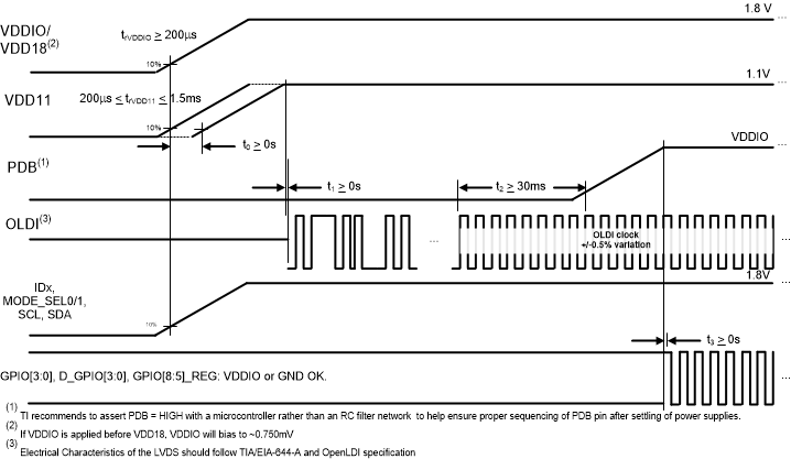
9.1 Power-Up Requirements and PDB Pin
The power supply ramp should be faster than 1.5 ms with a monotonic rise. A large capacitor on the PDB pin is needed to ensure PDB arrives after all the supply pins have settled to the recommended operating voltage. When PDB pin is pulled up to VDDIO, a 10-kΩ pull-up and a >10-μF capacitor to GND are required to delay the PDB input signal rise. All inputs must not be driven until all power supplies have reached steady state.
The recommended power up sequence is as follows:
- VDD18
- VDD11
- Wait until all supplies have settled
- Activate PDB
- Apply OpenLDI input
After power up write the following to the device:
Reg0x40=0x10 // select OLDI register
Reg0x41=0x49 // force PLL controller in PPM reset state
Reg0x42=0x16
Reg0x41=0x47 // force PLL LOCK Low
Reg0x42=0x20
Reg0x42=0xA0 // reset PLL divider
Reg0x42=0x20
Reg0x42=0x00 // release PLL LOCK control
Reg0x41=0x49 // release PLL state control
Reg0x42=0x00
 Figure 42. Recommended Power Sequencing