SNLS231P September   2006  – August 2024 DS90UR124-Q1 , DS90UR241-Q1

PRODUCTION DATA  

  1.   1
  2. 1Features
  3. 2Applications
  4. 3Description
  5. 4Pin Configuration and Functions
  6. 5Specifications
    1. 5.1 Absolute Maximum Ratings
    2. 5.2 ESD Ratings
    3. 5.3 Recommended Operating Conditions
    4. 5.4 Thermal Information
    5. 5.5 Electrical Characteristics
    6. 5.6 Serializer Input Timing Requirements for TCLK
    7. 5.7 Serializer Switching Characteristics
    8. 5.8 Deserializer Switching Characteristics
    9. 5.9 Typical Characteristics
  7. 6Detailed Description
    1. 6.1 Overview
    2. 6.2 Functional Block Diagram
    3. 6.3 Feature Description
      1. 6.3.1  Initialization and Locking Mechanism
      2. 6.3.2  Data Transfer
      3. 6.3.3  Resynchronization
      4. 6.3.4  Powerdown
      5. 6.3.5  Tri-State
      6. 6.3.6  Pre-Emphasis
      7. 6.3.7  AC-Coupling and Termination
        1. 6.3.7.1 Receiver Termination Option 1
        2. 6.3.7.2 Receiver Termination Option 2
        3. 6.3.7.3 Receiver Termination Option 3
      8. 6.3.8  Signal Quality Enhancers
      9. 6.3.9  @SPEED-BIST Test Feature
      10. 6.3.10 Backward-Compatible Mode With DS90C241 and DS90C124
    4. 6.4 Device Functional Modes
  8.   Application and Implementation
    1. 7.1 Application Information
      1. 7.1.1 Using the DS90UR241 and DS90UR124
      2. 7.1.2 Display Application
      3. 7.1.3 Typical Application Connection
    2. 7.2 Typical Applications
      1. 7.2.1 DS90UR241-Q1 Typical Application Connection
        1. 7.2.1.1 Design Requirements
        2. 7.2.1.2 Detailed Design Procedure
          1. 7.2.1.2.1 Power Considerations
          2. 7.2.1.2.2 Noise Margin
          3. 7.2.1.2.3 Transmission Media
          4. 7.2.1.2.4 46
          5. 7.2.1.2.5 Live Link Insertion
        3. 7.2.1.3 Application Curves
      2. 7.2.2 DS90UR124 Typical Application Connection
        1. 7.2.2.1 Design Requirements
        2. 7.2.2.2 Detailed Design Procedure
        3. 7.2.2.3 Application Curves
    3. 7.3 Power Supply Recommendations
    4. 7.4 Layout
      1. 7.4.1 Layout Guidelines
        1. 7.4.1.1 PCB Layout and Power System Considerations
        2. 7.4.1.2 LVDS Interconnect Guidelines
      2. 7.4.2 Layout Examples
  9. 7Device and Documentation Support
    1. 7.1 Device Support
    2. 7.2 Documentation Support
      1. 7.2.1 Related Documentation
    3. 7.3 Receiving Notification of Documentation Updates
    4. 7.4 Support Resources
    5. 7.5 Trademarks
    6. 7.6 Electrostatic Discharge Caution
    7. 7.7 Glossary
  10. 8Revision History
  11.   Mechanical, Packaging, and Orderable Information

Package Options

Mechanical Data (Package|Pins)
Thermal pad, mechanical data (Package|Pins)
Orderable Information

Description

The DS90URxxx-Q1 chipset translates a 24-bit parallel bus into a fully transparent data/control FPD-Link II LVDS serial stream with embedded clock information. This chipset is designed for driving graphical data to displays requiring 18-bit color depth: RGB666 + HS, VS, DE + three additional general-purpose data channels. This single serial stream simplifies transferring a 24-bit bus over PCB traces and cable by eliminating the skew problems between parallel data and clock paths. The device saves system cost by narrowing data paths that in turn reduce PCB layers, cable width, and connector size and pins.

The DS90URxxx-Q1 incorporates FPD-Link II LVDS signaling on the high-speed I/O. FPD-Link II LVDS provides a low-power and low-noise environment for reliably transferring data over a serial transmission path. By optimizing the Serializer output edge rate for the operating frequency range, EMI is further reduced.

In addition, the device features pre-emphasis to boost signals over longer distances using lossy cables. Internal DC-balanced encoding and decoding is used to support AC-coupled interconnects. Using TI’s proprietary random lock, the parallel data of the Serializer are randomized to the Deserializer without the need of REFCLK.

Device Information
PART NUMBER PACKAGE (1) BODY SIZE (NOM) (2)
DS90UR124-Q1 TQFP (64) 10.00mm × 10.00mm
DS90UR241-Q1 TQFP (48) 7.00mm × 7.00mm
For all available packages, see the orderable addendum at the end of the data sheet.
The package size (length × width) is a nominal value and includes pins, where applicable.
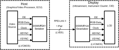
DS90UR124-Q1 DS90UR241-Q1 Applications DiagramApplications Diagram
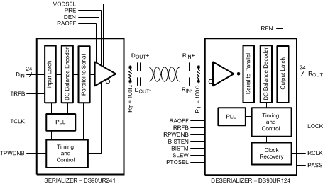
DS90UR124-Q1 DS90UR241-Q1 Block DiagramBlock Diagram