SNLS231P September 2006 – August 2024 DS90UR124-Q1 , DS90UR241-Q1
PRODUCTION DATA
- 1
- 1Features
- 2Applications
- 3Description
- 4Pin Configuration and Functions
- 5Specifications
-
6Detailed Description
- 6.1 Overview
- 6.2 Functional Block Diagram
- 6.3 Feature Description
- 6.4 Device Functional Modes
- Application and Implementation
- 7Device and Documentation Support
- 8Revision History
- Mechanical, Packaging, and Orderable Information
Package Options
Mechanical Data (Package|Pins)
- PFB|48
Thermal pad, mechanical data (Package|Pins)
Orderable Information
5.8 Deserializer Switching Characteristics
over recommended operating supply and temperature ranges unless otherwise specified
| PARAMETER | TEST CONDITIONS | PIN/FREQ. | MIN | TYP | MAX | UNIT | |
|---|---|---|---|---|---|---|---|
| tRCP | Receiver out Clock Period | tRCP = tTCP, PTOSEL = H | RCLK Figure 5-15 | 23.25 | T | 200 | ns |
| tRDC | RCLK Duty Cycle | PTOSEL = H, SLEW = L | 45% | 50% | 55% | ||
| tCLH | LVCMOS Low-to-High Transition Time | CL = 4pF (lumped load), SLEW = H | ROUT [0:23], RCLK, LOCK | 1.5 | 2.5 | ns | |
| tCHL | LVCMOS High-to-Low Transition Time | 1.5 | 2.5 | ns | |||
| tCLH | LVCMOS Low-to-High Transition Time | CL = 4pF (lumped load), SLEW = L | ROUT [0:23], RCLK, LOCK | 2.0 | 3.5 | ns | |
| tCHL | LVCMOS High-to-Low Transition Time | 2.0 | 3.5 | ns | |||
| tROS | ROUT (0:7) Setup Data to RCLK (Group 1) | PTOSEL = L, SLEW = H, Figure 5-16 | ROUT[0:7] | (0.35)× tRCP | (0.5×tRCP)–3 UI | ns | |
| tROH | ROUT (0:7) Hold Data to RCLK (Group 1) | (0.35)× tRCP | (0.5×tRCP)–3 UI | ns | |||
| tROS | ROUT (8:15) Setup Data to RCLK (Group 2) | PTOSEL = L, SLEW = H, Figure 5-16 | ROUT [8:15], LOCK | (0.35)× tRCP | (0.5×tRCP)–3 UI | ns | |
| tROH | ROUT (8:15) Hold Data to RCLK (Group 2) | (0.35)× tRCP | (0.5×tRCP)–3 UI | ns | |||
| tROS | ROUT (16:23) Setup Data to RCLK (Group 3) | ROUT [16:23] | (0.35)× tRCP | (0.5×tRCP)–3 UI | ns | ||
| tROH | ROUT (16:23) Setup Data to RCLK (Group 3) | (0.35)× tRCP | (0.5×tRCP)–3 UI | ns | |||
| tROS | ROUT (0:7) Setup Data to RCLK (Group 1) | PTOSEL = H, SLEW = H, Figure 5-15 | ROUT[0:7] | (0.35)× tRCP | (0.5×tRCP)–2 UI | ns | |
| tROH | ROUT (0:7) Hold Data to RCLK (Group 1) | (0.35)× tRCP | (0.5×tRCP)+2 UI | ns | |||
| tROS | ROUT (8:15) Setup Data to RCLK (Group 2) | ROUT [8:15], LOCK | (0.35)× tRCP | (0.5×tRCP)−1 UI | ns | ||
| tROH | ROUT (8:15) Hold Data to RCLK (Group 2) | (0.35)× tRCP | (0.5×tRCP)+1 UI | ns | |||
| tROS | ROUT (16:23) Setup Data to RCLK (Group 3) | ROUT [16:23] | (0.35)× tRCP | (0.5×tRCP)+1 UI | ns | ||
| tROH | ROUT (16:23) Setup Data to RCLK (Group 3) | (0.35)× tRCP | (0.5×tRCP)–1 UI | ns | |||
| tHZR | HIGH to Tri-state Delay | PTOSEL = H, Figure 5-14 | ROUT [0:23], RCLK, LOCK | 3 | 10 | ns | |
| tLZR | LOW to Tri-state Delay | 3 | 10 | ns | |||
| tZHR | Tri-state to HIGH Delay | 3 | 10 | ns | |||
| tZLR | Tri-state to LOW Delay | 3 | 10 | ns | |||
| tDD | Deserializer Delay | PTOSEL = H, Figure 5-12 | RCLK | [5+(5/56)]T+3.7 | [5+(5/56)]T +8 | ns | |
| tDSR | Deserializer PLL Lock Time from Powerdown | See Figure 5-14 | 5MHz | 128k*T | ms | ||
| 43MHz | 128k*T | ||||||
| RxIN_TOL-L | Receiver INput TOLerance Left | See Figure 5-17 | 5MHz–43MHz | 0.25 | UI | ||
| RxIN_TOL-R | Receiver INput TOLerance Right | See Figure 5-17 | 5MHz–43MHz | 0.25 | UI | ||
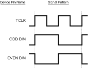 Figure 5-1 Serializer Input Checkerboard Pattern
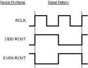 Figure 5-2 Deserializer Output Checkerboard Pattern
 Figure 5-3 Serializer LVDS Output Load and Transition Times
 Figure 5-4 Serializer Input Clock Transition Times
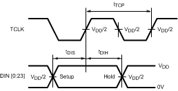 Figure 5-5 Serializer Setup and Hold Times
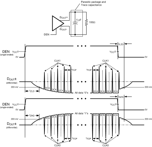 Figure 5-6 Serializer Tri-State Test Circuit and Delay
 Figure 5-7 Serializer PLL Lock Time, and TPWDNB Tri-State Delays
 Figure 5-8 Serializer Delay
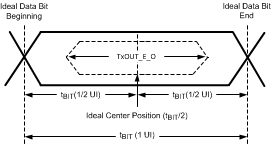 Figure 5-9 Transmitter Output Eye Opening (TxOUT_E_O)
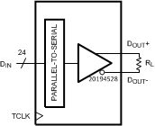
VOD = (DOUT+) – (DOUT−)
Differential output signal is shown as (DOUT+) – (DOUT−), device in Data Transfer mode.
Figure 5-10 Serializer VOD Diagram Figure 5-11 Deserializer LVCMOS Output Load and Transition Times
 Figure 5-12 Deserializer Delay
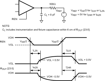 Figure 5-13 Deserializer Tri-State Test Circuit and Timing
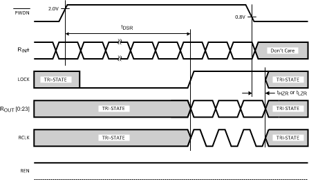 Figure 5-14 Deserializer PLL Lock Times and RPWDNB Tri-State Delay
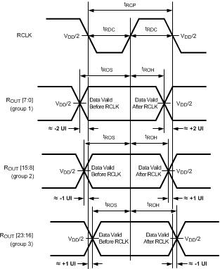 Figure 5-15 Deserializer Setup and Hold Times and PTO, PTOSEL = H
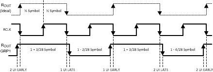
Group 1 will be latched internally by sequence of (early 2UI, late 1UI, early 1UI, late 2UI).
Group 2 will be latched internally by sequence of (late 1UI, early 1UI, late 2UI, early 2UI).
Group 3 will be latched internally by sequence of (early 1UI, late 2UI, early 2UI, late 1UI).
Figure 5-16 Deserializer Setup and Hold Times and PTO Spread, PTOSEL = L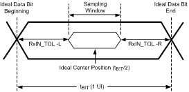
RxIN_TOL_L is the ideal noise margin on the left of the figure, with respect to ideal.
RxIN_TOL_R is the ideal noise margin on the right of the figure, with respect to ideal.
Figure 5-17 Receiver Input Tolerance (RxIN_TOL) and Sampling Window